What every programmer should know about memory, Part 1
SourceThis article brought to you by LWN subscribers
Subscribers to LWN.net made this article — and everything that surrounds it — possible. If you appreciate our content, please buy a subscription and make the next set of articles possible.
[Editor's introduction: Ulrich Drepper recently approached us asking if
we would be interested in publishing a lengthy document he had written on
how memory and software interact. We did not have to look at the text for
long to realize that it would be of interest to many LWN readers. Memory
usage is often the determining factor in how software performs, but good
information on how to avoid memory bottlenecks is hard to find. This
series of articles should change that situation.
The original document prints out at over 100 pages. We will be splitting
it into about seven segments, each run 1-2 weeks after its predecessor.
Once the entire series is out, Ulrich will be releasing the full text.
Reformatting the text from the original LaTeX has been a bit of a
challenge, but the results, hopefully, will be good. For ease of online
reading, Ulrich's footnotes have been placed {inline in the text}.
Hyperlinked cross-references (and [bibliography references]) will not be
possible until the full series is published.
Many thanks to Ulrich for allowing LWN to publish this material; we hope
that it will lead to more memory-efficient software across our systems in
the near future.
1 Introduction
In the early days computers were much simpler. The various components
of a system, such as the CPU, memory, mass storage, and network
interfaces, were developed together and, as a result, were quite
balanced in their performance. For example, the memory and network
interfaces were not (much) faster than the CPU at providing data.
This situation changed once the basic structure of computers
stabilized and hardware developers concentrated on optimizing
individual subsystems. Suddenly the performance of some components of
the computer fell significantly behind and bottlenecks developed.
This was especially true for mass storage and memory subsystems which,
for cost reasons, improved more slowly relative to other components.
The slowness of mass storage has mostly been dealt with using software
techniques: operating systems keep most often used (and most likely to
be used) data in main memory, which can be accessed at a rate orders of
magnitude faster than the hard disk. Cache storage was added to the
storage devices themselves, which requires no changes in the operating system to
increase performance. {Changes are needed, however, to
guarantee data integrity when using storage device caches.} For the
purposes of this paper, we will not go into more details of software
optimizations for the mass storage access.
Unlike storage subsystems, removing the main memory as a bottleneck
has proven much more difficult and almost all solutions require changes to
the hardware. Today these changes mainly come in the following forms:
- RAM hardware design (speed and parallelism).
- Memory controller designs.
- CPU caches.
- Direct memory access (DMA) for devices.
For the most part, this document will deal with CPU caches and some
effects of memory controller design. In the process of exploring
these topics, we will explore DMA and bring it into the larger
picture. However, we will start with an overview of the design for
today's commodity hardware. This is a prerequisite to understanding
the problems and the limitations of efficiently using memory
subsystems. We will also learn about, in some detail, the different types
of RAM and illustrate why these differences still exist.
This document is in no way all inclusive and final. It is limited to
commodity hardware and further limited to a subset of that hardware.
Also, many topics will be discussed in just enough detail
for the goals of this paper. For such topics, readers are recommended to
find more detailed documentation.
When it comes to operating-system-specific details and solutions,
the text exclusively
describes Linux. At no time will it contain any information about
other OSes. The author has no interest in discussing the implications
for other OSes. If the reader thinks s/he has to use a different OS
they have to go to their vendors and demand they write documents
similar to this one.
One last comment before the start. The text contains a number of
occurrences of the term “usually” and other, similar qualifiers.
The technology discussed here exists in many, many
variations in the real world and this paper only addresses the most
common, mainstream versions. It is rare that absolute statements can be
made about this technology, thus the qualifiers.
1.1 Document Structure
This document is mostly for software developers. It does not go into
enough technical details of the hardware to be useful for
hardware-oriented readers. But before we can go into the practical
information for developers a lot of groundwork must be laid.
To that end, the second section describes random-access memory (RAM) in
technical detail. This
section's content is nice to know but not absolutely critical to be able to
understand the later sections. Appropriate back references to the
section are added in places where the content is required so that the
anxious reader could skip most of this section at first.
The third section goes into a lot of details of CPU cache behavior.
Graphs have been used to keep the text from being as dry as it would otherwise
be. This content is essential for an understanding of the rest of the document.
Section 4 describes briefly how virtual memory is implemented. This
is also required groundwork for the rest.
Section 5 goes into a lot of detail about Non Uniform Memory
Access (NUMA) systems.
Section 6 is the central section of this paper. It brings together
all the previous sections' information and gives programmers advice on
how to write code which performs well in the various situations. The
very impatient reader could start with this section and, if necessary, go
back to the earlier sections to freshen up the knowledge of the
underlying technology.
Section 7 introduces tools which can help the programmer do a
better job. Even with a complete understanding of the technology it
is far from obvious where in a non-trivial software project the
problems are. Some tools are necessary.
In section 8 we finally give an outlook of technology which can be
expected in the near future or which might just simply be good to have.
1.2 Reporting Problems
The author intends to update this document for some time. This
includes updates made necessary by advances in technology but also to
correct mistakes. Readers willing to report problems are encouraged
to send email.
1.3 Thanks
I would like to thank Johnray Fuller and especially Jonathan Corbet for taking on part of the
daunting task of transforming the author's form of English into something
more traditional. Markus Armbruster provided a lot of valuable input
on problems and omissions in the text.
1.4 About this Document
The title of this paper is an homage to David Goldberg's classic paper
“What Every Computer Scientist Should Know About Floating-Point
Arithmetic” [goldberg]. Goldberg's paper is still not widely
known, although it should be a prerequisite for anybody daring to
touch a keyboard for serious programming.
Understanding commodity hardware is important because specialized
hardware is in retreat. Scaling these days is most often achieved
horizontally instead of vertically, meaning today it is more cost-effective
to use many smaller, connected commodity computers
instead of a few really large and exceptionally fast (and expensive)
systems. This is the case because fast and inexpensive network
hardware is widely available. There are still situations where the
large specialized systems have their place and these systems still
provide a business opportunity, but the overall market is dwarfed by
the commodity hardware market. Red Hat, as of 2007, expects that for
future products, the “standard building blocks” for most data
centers will be a computer with up to four sockets, each filled with a
quad core CPU that, in the case of Intel CPUs, will be
hyper-threaded. {Hyper-threading enables a single processor core to be used for two or more concurrent executions with just a little extra hardware.} This means the standard system in the data
center will have up to 64 virtual processors. Bigger machines will be
supported, but the quad socket, quad CPU core case is currently
thought to be the sweet spot and most optimizations are targeted for
such machines.
Large differences exist in the structure of commodity computers. That
said, we will cover more than 90% of such hardware by concentrating
on the most important differences. Note that these technical details
tend to change rapidly, so the reader is advised to take the date
of this writing into account.
Over the years the personal computers and smaller servers standardized
on a chipset with two parts: the Northbridge and Southbridge.
Figure 2.1 shows this structure.
Figure 2.1: Structure with Northbridge and Southbridge
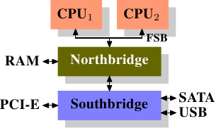
All CPUs (two in the previous example, but there can be more) are
connected via a common bus (the Front Side Bus, FSB) to the
Northbridge. The Northbridge contains, among other things, the memory
controller, and its implementation determines the type of RAM chips
used for the computer. Different types of RAM, such as DRAM, Rambus,
and SDRAM, require different memory controllers.
To reach all other system devices, the Northbridge must communicate with
the Southbridge. The Southbridge, often referred to as the I/O
bridge, handles communication with devices through a variety of
different buses. Today the PCI, PCI Express, SATA, and USB buses are
of most importance, but PATA, IEEE 1394, serial, and parallel ports
are also supported by the Southbridge. Older systems had AGP slots
which were attached to the Northbridge. This was done for performance
reasons related to insufficiently fast connections between the
Northbridge and Southbridge. However, today the PCI-E slots are all
connected to the Southbridge.
Such a system structure has a number of noteworthy consequences:
- All data communication from one CPU to another must travel over the same bus used to communicate with the Northbridge.
- All communication with RAM must pass through the Northbridge.
- The RAM has only a single port.
{We will not discuss multi-port RAM in this document as this
type of RAM is not found in commodity hardware, at least not in places
where the programmer has access to it. It can be found in specialized
hardware such as network routers which depend on utmost speed.} - Communication between a CPU and a device attached to the Southbridge is routed through the Northbridge.
A couple of bottlenecks are immediately apparent in this design. One
such bottleneck involves access to RAM for devices. In the earliest
days of the PC, all communication with devices on either bridge had to
pass through the CPU, negatively impacting overall system performance.
To work around this problem some devices became capable of direct
memory access (DMA). DMA allows devices, with the help of the
Northbridge, to store and receive data in RAM directly without the
intervention of the CPU (and its inherent performance cost). Today all
high-performance devices attached to any of the buses can utilize DMA.
While this greatly reduces the workload on the CPU, it also creates
contention for the bandwidth of the Northbridge as DMA requests
compete with RAM access from the CPUs. This problem, therefore, must
to be taken into account.
A second bottleneck involves the bus from the Northbridge to the RAM.
The exact details of the bus depend on the memory types deployed.
On older systems there is only one bus to all the RAM chips, so
parallel access is not possible. Recent RAM types require
two separate buses (or channels as they are called for DDR2,
see Figure 2.8) which doubles the available bandwidth. The
Northbridge interleaves memory access across the channels. More
recent memory technologies (FB-DRAM, for instance) add more channels.
With limited bandwidth available, it is important to schedule memory
access in ways that minimize delays. As we will see, processors are much faster and
must wait to access memory, despite the use of CPU caches. If multiple
hyper-threads, cores, or processors access memory at the same time,
the wait times for memory access are even longer. This is also true
for DMA operations.
There is more to accessing memory than
concurrency, however. Access patterns themselves also greatly
influence the performance of the memory subsystem, especially with
multiple memory channels. Refer to Section 2.2 for more
details of RAM access patterns.
On some more expensive systems, the Northbridge does not actually
contain the memory controller. Instead the Northbridge can be
connected to a number of external memory controllers (in the following
example, four of them).
Figure 2.2: Northbridge with External Controllers
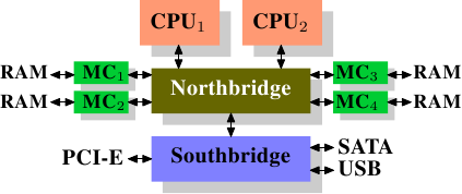
The advantage of this architecture is that more than one memory bus
exists and therefore total bandwidth increases. This design also
supports more memory. Concurrent memory access patterns reduce delays
by simultaneously accessing different memory banks. This is
especially true when multiple processors are directly connected to
the Northbridge, as in Figure 2.2. For such a design, the
primary limitation is the internal bandwidth of the Northbridge, which
is phenomenal for this architecture (from Intel). {For
completeness it should be mentioned that such a memory controller
arrangement can be used for other purposes such as “memory RAID”
which is useful in combination with hotplug memory.}
Using multiple external memory controllers is not the only way to
increase memory bandwidth. One other increasingly popular way is to integrate
memory controllers into the CPUs and attach memory to each CPU. This
architecture is made popular by SMP systems based on AMD's Opteron
processor. Figure 2.3 shows such a system. Intel will have
support for the Common System Interface (CSI) starting with the
Nehalem processors; this is basically the same approach: an integrated
memory controller with the possibility of local memory for each
processor.
Figure 2.3: Integrated Memory Controller
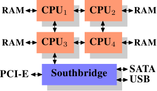
With an architecture like this there are as many memory banks
available as there are processors. On a quad-CPU machine the memory
bandwidth is quadrupled without the need for a complicated Northbridge with
enormous bandwidth. Having a memory controller integrated into the
CPU has some additional advantages; we will not dig deeper into this
technology here.
There are disadvantages to this architecture, too. First of all,
because the machine still has to make all the memory of the system
accessible to all processors, the memory is not uniform anymore (hence
the name NUMA - Non-Uniform Memory Architecture - for such an architecture).
Local memory (memory attached to a processor)
can be accessed with the usual speed. The situation is different when
memory attached to another processor is accessed. In this case
the interconnects between the processors have to be used. To access
memory attached to CPU2 from CPU1 requires communication across one
interconnect. When the same CPU accesses memory attached to
CPU4 two interconnects have to be crossed.
Each such communication has an associated cost. We talk about “NUMA
factors” when we describe the extra time needed to access remote
memory. The example architecture in Figure 2.3 has two
levels for each CPU: immediately adjacent CPUs and one CPU
which is two interconnects away. With more
complicated machines the number of levels can grow significantly. There are
also machine architectures (for instance IBM's x445 and SGI's
Altix series) where there is more than one type of connection. CPUs
are organized into nodes; within a node the time to access the
memory might be uniform or have only small NUMA factors. The
connection between nodes can be very expensive, though, and the NUMA
factor can be quite high.
Commodity NUMA machines exist today and will likely play an even greater
role in the future. It is expected that, from late 2008 on, every SMP
machine will use NUMA. The costs associated with NUMA make it important to
recognize when a program is running on a NUMA machine. In
Section 5 we will discuss more machine architectures and some
technologies the Linux kernel provides for these programs.
Beyond the technical details described in the remainder of this
section, there are several additional factors which influence the
performance of RAM. They are not controllable by software, which is
why they are not covered in this section. The interested reader can
learn about some of these factors in Section 2.1. They are really
only needed to get a more complete picture of RAM technology and
possibly to make better decisions when purchasing computers.
The following two sections discuss hardware details at the gate level
and the access protocol between the memory controller and the DRAM
chips. Programmers will likely find this information enlightening since these
details explain why RAM access works the way it does. It is optional
knowledge, though, and the reader anxious to get to topics with more
immediate relevance for everyday life can jump ahead to
Section 2.2.5.
2.1 RAM Types
There have been many types of RAM over the years and each type
varies, sometimes significantly, from the other. The older types are
today really only interesting to the historians. We will not explore
the details of those. Instead we will concentrate on modern RAM types;
we will only scrape the surface, exploring some details which are
visible to the kernel or application developer through their
performance characteristics.
The first interesting details are centered around the question why
there are different types of RAM in the same machine. More
specifically, why there are both static RAM (SRAM {In other contexts
SRAM might mean “synchronous RAM”.}) and dynamic RAM (DRAM). The
former is much faster and provides the same functionality. Why is not
all RAM in a machine SRAM? The answer is, as one might expect, cost.
SRAM is much more expensive to produce and to use than DRAM. Both
these cost factors are important, the second one increasing in
importance more and more. To understand these difference we look at
the implementation of a bit of storage for both SRAM and DRAM.
In the remainder of this section we will discuss some low-level
details of the implementation of RAM. We will keep the level of detail as
low as possible. To that end, we will discuss the signals at a “logic level” and not at
a level a hardware designer would have to use. That level of detail
is unnecessary for our purpose here.
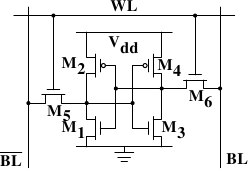
2.1.1 Static RAM
Figure 2.4: 6-T Static RAM
Read Next page