What every programmer should know about memory, Part 1
Source
Figure 2.4 shows the structure of a 6 transistor SRAM cell.
The core of this cell is formed by the four transistors M1
to M4 which form two cross-coupled inverters. They have
two stable states, representing 0 and 1 respectively. The state is
stable as long as power on Vdd is available.
If access to the state of the cell is needed the word access line
WL is raised. This makes the state of the cell immediately
available for reading on BL and
BL. If the cell state must be
overwritten the BL and BL
lines are first set to the desired values and then WL is
raised. Since the outside drivers are stronger than the four
transistors (M1 through M4) this
allows the old state to be overwritten.
See [sramwiki] for a more detailed description of the way the cell works.
For the following discussion it is important to note that
- one cell requires six transistors. There are variants with four transistors but they have disadvantages.
- maintaining the state of the cell requires constant power.
- the cell state is available for reading almost immediately once the word access line WL is raised. The signal is as rectangular (changing quickly between the two binary states) as other transistor-controlled signals.
- the cell state is stable, no refresh cycles are needed.
There are other, slower and less power-hungry, SRAM forms available, but
those are not of interest here since we are looking at fast RAM.
These slow variants are mainly interesting because they can be more
easily used in a system than dynamic RAM because of their
simpler interface.
2.1.2 Dynamic RAM
Dynamic RAM is, in its structure, much simpler than static RAM.
Figure 2.5 shows the structure of a usual DRAM cell design.
All it consists of is one transistor and one capacitor. This huge
difference in complexity of course means that it functions very differently
than static RAM.
Figure 2.5: 1-T Dynamic RAM
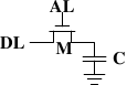
A dynamic RAM cell keeps its state in the capacitor C. The
transistor M is used to guard the access to the state. To
read the state of the cell the access line AL is raised;
this either causes a current to flow on the data line DL or
not, depending on the charge in the capacitor. To write to the cell the
data line DL is appropriately set and then AL is raised for a time long enough to charge or
drain the capacitor.
There are a number of complications with the design of dynamic RAM.
The use of a capacitor means that reading the cell discharges the
capacitor. The procedure cannot be repeated indefinitely, the
capacitor must be recharged at some point. Even worse, to accommodate
the huge number of cells (chips with 109 or more cells are now
common) the capacity to the capacitor must be low (in the femto-farad range
or lower). A fully charged capacitor holds a few 10's of thousands of
electrons. Even though the resistance of the capacitor is high (a
couple of tera-ohms) it only takes a short time for the capacity to
dissipate. This problem is called “leakage”.
This leakage is why a DRAM cell must be constantly refreshed. For most DRAM
chips these days this refresh must happen every 64ms. During the refresh cycle no access to
the memory is possible. For some workloads this overhead might stall
up to 50% of the memory accesses (see [highperfdram]).
A second problem resulting from the tiny charge is that the
information read from the cell is not directly usable. The data line
must be connected to a sense amplifier which can distinguish between
a stored 0 or 1 over the whole range of charges which still have to
count as 1.
A third problem is that charging and draining a capacitor is not
instantaneous. The signals received by the sense amplifier are not
rectangular, so a conservative estimate as to when the output of the
cell is usable has to be used. The formulas for charging and
discharging a capacitor are
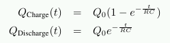
This means it takes some time (determined by the capacity C and
resistance R) for the capacitor to be charged and discharged. It also
means that the current which can be detected by the sense amplifiers
is not immediately available. Figure 2.6 shows the charge and
discharge curves. The X—axis is measured in units of RC (resistance
multiplied by capacitance) which is a unit of time.
Figure 2.6: Capacitor Charge and Discharge Timing
Unlike the static RAM case where the output is immediately available when
the word access line is raised, it will always take a bit of time until the
capacitor discharges sufficiently. This delay severely limits how fast
DRAM can be.
The simple approach has its advantages, too. The main advantage is
size. The chip real estate needed for one DRAM cell is many times
smaller than that of an SRAM cell. The SRAM cells also need
individual power for the transistors maintaining the state. The
structure of the DRAM cell is also simpler and more regular which
means packing many of them close together on a die is simpler.
Overall, the (quite dramatic) difference in cost wins. Except in
specialized hardware — network routers, for example — we have to live with main memory
which is based on DRAM. This has huge implications on the programmer
which we will discuss in the remainder of this paper. But first we need
to look into a few more details of the actual use of DRAM cells.
2.1.3 DRAM Access
A program selects a memory location using a virtual address. The
processor translates this into a physical address and finally the
memory controller selects the RAM chip corresponding to that address. To
select the individual memory cell on the RAM chip, parts of the
physical address are passed on in the form of a number of address
lines.
It would be completely impractical to address memory locations
individually from the memory controller: 4GB of RAM would require
232 address lines.
Instead the address is passed encoded as a binary number using a
smaller set of address lines. The address passed to the DRAM chip
this way must be demultiplexed first. A demultiplexer with N
address lines will have 2N output lines. These output lines can be
used to select the memory cell. Using this direct approach is no big
problem for chips with small capacities.
But if the number of cells grows this approach is not suitable
anymore. A chip with 1Gbit
{I hate those SI prefixes. For me
a giga-bit will always be 230 and not 109 bits.} capacity
would need 30 address lines and 230 select lines. The size of a
demultiplexer increases exponentially with the number of input lines
when speed is not to be sacrificed. A demultiplexer for 30 address
lines needs a whole lot of chip real estate in addition to the
complexity (size and time) of the demultiplexer. Even more
importantly, transmitting 30 impulses on the address lines
synchronously is much harder than transmitting “only” 15 impulses.
Fewer lines have to be laid out at exactly the same length or timed
appropriately. {Modern DRAM types like DDR3 can automatically
adjust the timing but there is a limit as to what can be tolerated.}
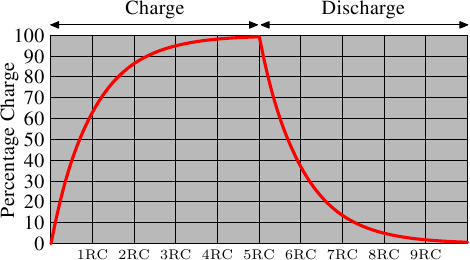
Figure 2.7: Dynamic RAM Schematic
Figure 2.7 shows a DRAM chip at a very high level. The DRAM
cells are organized in rows and columns. They could all be aligned in
one row but then the DRAM chip would need a huge demultiplexer. With
the array approach the design can get by with one demultiplexer and
one multiplexer of half the size. {Multiplexers and
demultiplexers are equivalent and the multiplexer here needs to work
as a demultiplexer when writing. So we will drop the differentiation
from now on.} This is a huge saving on all fronts. In the example
the address lines a0 and
a1 through the row address
selection (RAS)
demultiplexer select the address lines of a whole row of cells. When
reading, the content of all cells is thusly made available to the
column address selection (CAS)
{The line over the name
indicates that the signal is negated} multiplexer. Based on the
address lines a2 and
a3 the content of one column is
then made available to the data pin of the DRAM chip. This happens
many times in parallel on a number of DRAM chips to produce a total
number of bits corresponding to the width of the data bus.
For writing, the new cell value is put on the data bus and, when the
cell is selected using the RAS and CAS, it is stored in the cell.
A pretty straightforward design. There are in reality — obviously — many
more complications. There need to be specifications for how much delay there
is after the signal before the data will be available on the data bus for
reading. The capacitors do not unload instantaneously, as described
in the previous section. The signal from the cells is so weak that
it needs to be amplified. For writing it must be specified how long
the data must be available on the bus after the RAS and CAS is
done to successfully store the new value in the cell (again, capacitors
do not fill or drain instantaneously). These timing constants are
crucial for the performance of the DRAM chip. We will talk about this
in the next section.
A secondary scalability problem is that having 30 address lines
connected to every RAM chip is not feasible either. Pins of a chip
are a precious resources. It is “bad” enough that the data must be
transferred as much as possible in parallel (e.g., in 64 bit batches).
The memory controller must be able to address each RAM module
(collection of RAM chips). If parallel access to multiple RAM modules
is required for performance reasons and each RAM module requires its own
set of 30 or more address lines, then the memory controller needs to
have, for 8 RAM modules, a whopping 240+ pins only for the address
handling.
To counter these secondary scalability problems DRAM chips have, for a long
time, multiplexed the address itself. That means the address is
transferred in two parts. The first part consisting of address bits
a0 and
a1 in the example in
Figure 2.7) select the row. This selection remains active
until revoked. Then the second part, address bits
a2 and
a3, select the column. The
crucial difference is that only two external address lines are needed.
A few more lines are needed to indicate when the RAS and CAS signals
are available but this is a small price to pay for cutting the number
of address lines in half. This address multiplexing brings its own
set of problems, though. We will discuss them in Section 2.2.
2.1.4 Conclusions
Do not worry if the details in this section are a bit overwhelming.
The important things to take away from this section are:
- there are reasons why not all memory is SRAM
- memory cells need to be individually selected to be used
- the number of address lines is directly responsible for the cost of the memory controller, motherboards, DRAM module, and DRAM chip
- it takes a while before the results of the read or write operation are available
The following section will go into more details about the actual
process of accessing DRAM memory. We are not going into more details
of accessing SRAM, which is usually directly addressed. This happens
for speed and because the SRAM memory is limited in size. SRAM is
currently used in CPU caches and on-die where the connections are small
and fully under control of the CPU designer. CPU caches are a topic
which we discuss later but all we need to know is that SRAM cells have
a certain maximum speed which depends on the effort spent on the
SRAM. The speed can vary from only slightly slower than the CPU core
to one or two orders of magnitude slower.
2.2 DRAM Access Technical Details
In the section introducing DRAM we saw that DRAM chips multiplex the
addresses in order to save resources. We also saw that accessing DRAM
cells takes time since the capacitors in those cells do not discharge instantaneously
to produce a stable signal; we also saw that DRAM cells must be
refreshed. Now it is time to put this all together and see how all
these factors determine how the DRAM access has to happen.
We will concentrate on current technology; we will not discuss
asynchronous DRAM and its variants as they are simply not relevant
anymore. Readers interested in this topic are referred to
[highperfdram] and [arstechtwo]. We will also not talk about
Rambus DRAM (RDRAM) even though the technology is not obsolete. It is just not widely used for system
memory. We will concentrate exclusively
on Synchronous DRAM (SDRAM) and its successors Double Data Rate DRAM
(DDR).
Synchronous DRAM, as the name suggests, works relative to a time
source. The memory controller provides a clock, the frequency of
which determines the speed of the Front Side Bus (FSB) —
the memory controller interface used by the DRAM chips. As of this writing,
frequencies of 800MHz, 1,066MHz, or even 1,333MHz are available with
higher frequencies (1,600MHz) being announced for the next generation. This
does not mean the frequency used on the bus is actually this high.
Instead, today's buses are double- or quad-pumped, meaning that data is
transported two or four times per cycle. Higher numbers sell so the
manufacturers like to advertise a quad-pumped 200MHz bus as an
“effective” 800MHz bus.
For SDRAM today each data transfer consists of 64 bits — 8 bytes. The
transfer rate of the FSB is therefore 8 bytes multiplied by the effective
bus frequency (6.4GB/s for the quad-pumped 200MHz bus). That sounds like a
lot but it is the burst speed, the maximum speed which will never be
surpassed. As we will see now the protocol for talking
to the RAM modules has a lot of downtime when no data can be transmitted.
It is exactly this downtime which we must understand and minimize to
achieve the best performance.
2.2.1 Read Access Protocol
Figure 2.8: SDRAM Read Access Timing
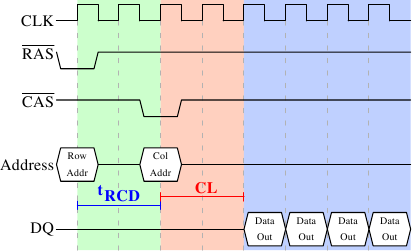
Figure 2.8 shows the activity on some of the connectors of
a DRAM module which happens in three differently colored phases. As
usual, time flows from left to right. A lot of details are left out.
Here we only talk about the bus clock, RAS and CAS signals, and
the address and data buses. A read cycle begins with the memory
controller making the row address available on the address bus and
lowering the RAS signal. All signals are read on the rising edge
of the clock (CLK) so it does not matter if the signal is not
completely square as long as it is stable at the time it is read.
Setting the row address causes the RAM chip to start latching the
addressed row.
The CAS signal can be sent after tRCD (RAS-to-CAS Delay)
clock cycles. The column address is then transmitted by making it
available on the address bus and lowering the CAS line. Here we
can see how the two parts of the address (more or less halves, nothing
else makes sense) can be transmitted over the same address bus.
Now the addressing is complete and the data can be transmitted. The
RAM chip needs some time to prepare for this. The delay is usually
called CAS Latency (CL). In Figure 2.8 the CAS
latency is 2. It can be higher or lower, depending on the quality of
the memory controller, motherboard, and DRAM module. The latency can
also have half values. With CL=2.5 the first data would be available
at the first falling flank in the blue area.
With all this preparation to get to the data it would be wasteful to
only transfer one data word. This is why DRAM modules allow the
memory controller to specify how much data is to be transmitted.
Often the choice is between 2, 4, or 8 words. This allows filling
entire lines in the caches without a new RAS/CAS sequence. It is also
possible for the memory controller to send a new CAS signal without
resetting the row selection. In this way, consecutive memory addresses
can be read from or written to significantly faster because the RAS signal does not have to be sent and the row does
not have to be deactivated (see below). Keeping the row “open” is
something the memory controller has to decide. Speculatively leaving
it open all the time has disadvantages with real-world applications
(see [highperfdram]). Sending new CAS signals is only subject
to the Command Rate of the RAM module (usually specified as Tx,
where x is a value like 1 or 2; it will be 1 for high-performance DRAM
modules which accept new commands every cycle).
In this example the SDRAM spits out one word per cycle. This is what
the first generation does. DDR is able to transmit two words per
cycle. This cuts down on the transfer time but does not change the
latency. In principle, DDR2 works the same although in practice it
looks different. There is no need to go into the details here. It is
sufficient to note that DDR2 can be made faster, cheaper, more
reliable, and is more energy efficient (see [ddrtwo] for more
information).
2.2.2 Precharge and Activation
Figure 2.8 does not cover the whole cycle. It only shows
parts of the full cycle of accessing DRAM. Before a new RAS signal
can be sent the currently latched row must be deactivated and the new
row must be precharged. We can concentrate here on the case where
this is done with an explicit command. There are improvements to the
protocol which, in some situations, allows this extra step to be avoided. The
delays introduced by precharging still affect the operation, though.
Figure 2.9: SDRAM Precharge and Activation
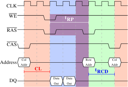
Figure 2.9 shows the activity starting from one CAS
signal to the CAS signal for another row. The data requested with
the first CAS signal is available as before, after CL cycles. In the
example two words are requested which, on a simple SDRAM, takes two
cycles to transmit. Alternatively, imagine four words on a DDR chip.
Even on DRAM modules with a command rate of one the precharge command
cannot be issued right away. It is necessary to wait as long as it
takes to transmit the data. In this case it takes two cycles. This
happens to be the same as CL but that is just a coincidence. The
precharge signal has no dedicated line; instead, some implementations
issue it by
lowering the Write Enable (WE) and RAS line simultaneously. This
combination has no useful meaning by itself (see [micronddr] for
encoding details).
Once the precharge command is issued it takes tRP (Row Precharge
time) cycles until the row can be selected. In Figure 2.9
much of the time (indicated by the purplish color) overlaps with the
memory transfer (light blue). This is good! But tRP is larger than
the transfer time and so the next RAS signal is stalled for one
cycle.
If we were to continue the timeline in the diagram we would find that
the next data transfer happens 5 cycles after the previous one stops.
This means the data bus is only in use two cycles out of seven.
Multiply this with the FSB speed and the theoretical 6.4GB/s for a
800MHz bus become 1.8GB/s. That is bad and must be avoided. The
techniques described in Section 6 help to raise this number.
But the programmer usually has to do her share.
There is one more timing value for a SDRAM module which we have not
discussed. In Figure 2.9 the precharge command was only
limited by the data transfer time. Another constraint is that an
SDRAM module needs time after a RAS signal before it can precharge
another row (denoted as tRAS). This number is usually pretty high,
in the order of two or three times the tRP value. This is a
problem if, after a RAS signal, only one CAS signal follows
and the data transfer is finished in a few cycles. Assume that in
Figure 2.9 the initial CAS signal was preceded directly
by a RAS signal and that tRAS is 8 cycles. Then the precharge
command would have to be delayed by one additional cycle since the sum of
tRCD, CL, and tRP (since it is larger than the data transfer time)
is only 7 cycles.
DDR modules are often described using a special notation: w-x-y-z-T.
For instance: 2-3-2-8-T1. This means:
w 2 CAS Latency (CL) x 3 RAS-to-CAS delay (tRCD) y 2 RAS
Precharge (tRP) z 8 Active to Precharge delay (tRAS) T T1 Command Rate
There are numerous other timing constants which affect the way
commands can be issued and are handled. Those five constants are in
practice sufficient to determine the performance of the module, though.
It is sometimes useful to know this information for the computers in
use to be able to interpret certain measurements. It is
definitely useful to know these details when buying computers since
they, along with the FSB and SDRAM module speed, are
among the most important factors determining a computer's speed.
Read Next page