What every programmer should know about memory, Part 1
Source
The very adventurous reader could also try to tweak a system.
Sometimes the BIOS allows changing some or all these values. SDRAM
modules have programmable registers where these values can be set.
Usually the BIOS picks the best default value. If the quality of the
RAM module is high it might be possible to reduce the one or the other
latency without affecting the stability of the computer. Numerous
overclocking websites all around the Internet provide ample of
documentation for doing this. Do it at your own risk, though and do not say
you have not been warned.
2.2.3 Recharging
A mostly-overlooked topic when it comes to DRAM access is recharging.
As explained in Section 2.1.2, DRAM cells must constantly be refreshed.
This does not happen completely transparently for the rest of the
system. At times when a row {Rows are the granularity this
happens with despite what [highperfdram] and other literature
says (see [micronddr]).} is recharged no access is possible. The
study in [highperfdram] found that “[s]urprisingly, DRAM
refresh organization can affect performance dramatically”.
Each DRAM cell must be refreshed every 64ms according to the JEDEC
specification. If a DRAM array has 8,192 rows this means the memory
controller has to issue a refresh command on average every
7.8125µs (refresh commands can be queued so in practice the
maximum interval between two requests can be higher). It is the
memory controller's responsibility to schedule the refresh commands.
The DRAM module keeps track of the address of the last refreshed row
and automatically increases the address counter for each new request.
There is really not much the programmer can do about the refresh and
the points in time when the commands are issued. But it is important
to keep this part to the DRAM life cycle in mind when interpreting
measurements. If a critical word has to be retrieved from a row which
currently is being refreshed the processor could be stalled for quite a long
time. How long each refresh takes depends on the DRAM module.
2.2.4 Memory Types
It is worth spending some time on the current and soon-to-be current
memory types in use. We will start with SDR (Single Data Rate) SDRAMs
since they are the basis of the DDR (Double Data Rate) SDRAMs. SDRs
were pretty simple. The memory cells and the data transfer rate were
identical.
Figure 2.10: SDR SDRAM Operation
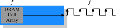
In Figure 2.10 the DRAM cell array can output the memory content at
the same rate it can be transported over the memory bus. If the DRAM
cell array can operate at 100MHz, the data transfer rate of the bus is thus
100Mb/s. The frequency f for all components is the same.
Increasing the throughput of the DRAM chip is expensive since the
energy consumption rises with the frequency. With a huge number of
array cells this is prohibitively expensive. {Power = Dynamic
Capacity × Voltage2 × Frequency.} In reality it is
even more of a problem since increasing the frequency usually also
requires increasing the voltage to maintain stability of the system.
DDR SDRAM (called DDR1
retroactively) manages to improve the throughput without increasing
any of the involved frequencies.
Figure 2.11: DDR1 SDRAM Operation
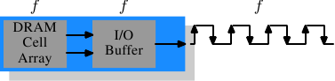
The difference between SDR and DDR1 is, as can be seen in
Figure 2.11 and guessed from the name, that twice the amount of
data is transported per cycle. I.e., the DDR1 chip transports data on
the rising and falling edge. This is sometimes called a
“double-pumped” bus. To make this possible without increasing the
frequency of the cell array a buffer has to be introduced. This
buffer holds two bits per data line. This in turn requires that, in
the cell array in Figure 2.7, the data bus consists of two
lines. Implementing this is trivial: one only has the use the same
column address for two DRAM cells and access them in parallel. The
changes to the cell array to implement this are also minimal.
The SDR
DRAMs were known simply by their frequency (e.g., PC100 for 100MHz
SDR). To make DDR1 DRAM sound better the marketers had to come up
with a new scheme since the frequency did not change. They came with
a name which contains the transfer rate in bytes a DDR module (they
have 64-bit busses) can sustain:
100MHz × 64bit × 2 = 1,600MB/s
Hence a DDR module with 100MHz frequency is called PC1600. With 1600
> 100 all marketing requirements are fulfilled; it sounds much
better although the improvement is really only a factor of
two. {I will take the factor of two but I do not have to like the inflated numbers.}
Figure 2.12: DDR2 SDRAM Operation
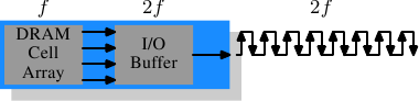
To get even more out of the memory technology DDR2 includes a bit more
innovation. The most obvious change that can be seen in
Figure 2.12 is the doubling of the frequency of the bus.
Doubling the frequency means doubling the bandwidth. Since this
doubling of the frequency is not economical for the cell array it is
now required that the I/O buffer gets four bits in each clock cycle
which it then can send on the bus. This means the changes to the DDR2
modules consist of making only the I/O buffer component of the DIMM
capable of running at higher speeds. This is certainly possible and
will not require measurably more energy, it is just one tiny component and
not the whole module. The names the marketers came up with for DDR2
are similar to the DDR1 names only in the computation of the value the
factor of two is replaced by four (we now have a quad-pumped bus).
Figure 2.13 shows the names of the modules in use today.
Array
Freq.
Bus
Freq.
Data
Rate
Name
(Rate)
Name
(FSB) 133MHz 266MHz 4,256MB/s PC2-4200 DDR2-533
166MHz 333MHz 5,312MB/s PC2-5300 DDR2-667
200MHz 400MHz 6,400MB/s PC2-6400 DDR2-800
250MHz 500MHz 8,000MB/s PC2-8000 DDR2-1000
266MHz 533MHz 8,512MB/s PC2-8500 DDR2-1066Figure 2.13: DDR2 Module Names
There is one more twist to the naming. The FSB speed used by CPU,
motherboard, and DRAM module is specified by using the
effective frequency. I.e., it factors in the transmission on both flanks of the clock cycle and thereby inflates
the number. So, a 133MHz module with a 266MHz bus has an FSB
“frequency” of 533MHz.
The specification for DDR3 (the real one, not the fake GDDR3 used in
graphics cards) calls for more changes along the lines of the
transition to DDR2. The voltage will be reduced from 1.8V
for DDR2 to 1.5V for DDR3. Since the power consumption equation is
calculated using the square of the voltage this alone brings a
30% improvement. Add to this a reduction in die size plus other
electrical advances and DDR3 can manage, at the same frequency, to get
by with half the power consumption. Alternatively, with higher
frequencies, the same power envelope can be hit. Or with double the
capacity the same heat emission can be achieved.
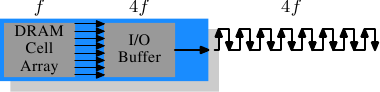
The cell array of DDR3 modules will run at a quarter of the speed of
the external bus which requires an 8 bit I/O buffer, up from 4 bits
for DDR2. See Figure 2.14 for the schematics.
Figure 2.14: DDR3 SDRAM Operation
Initially DDR3 modules will likely have slightly higher CAS
latencies just because the DDR2 technology is more mature. This would
cause DDR3 to be useful only at frequencies which are higher than those
which can be achieved with DDR2, and, even then, mostly when bandwidth is more
important than latency. There is already talk about 1.3V modules
which can achieve the same CAS latency as DDR2. In any case, the
possibility of achieving higher speeds because of faster buses will
outweigh the increased latency.
One possible problem with DDR3 is that, for 1,600Mb/s transfer rate or
higher, the number of modules per channel may be reduced to just one.
In earlier versions this requirement held for all frequencies, so one can hope that the requirement will at some point be lifted for all
frequencies. Otherwise the capacity of systems will be severely limited.
Figure 2.15 shows the names of the expected DDR3 modules.
JEDEC agreed so far on the first four types. Given that Intel's 45nm
processors have an FSB speed of 1,600Mb/s, the 1,866Mb/s is needed for
the overclocking market. We will likely see more of this towards the end
of the DDR3 lifecycle.
Array
Freq.
Bus
Freq.
Data
Rate
Name
(Rate)
Name
(FSB) 100MHz 400MHz 6,400MB/s PC3-6400 DDR3-800
133MHz 533MHz 8,512MB/s PC3-8500 DDR3-1066
166MHz 667MHz 10,667MB/s PC3-10667 DDR3-1333
200MHz 800MHz 12,800MB/s PC3-12800 DDR3-1600
233MHz 933MHz 14,933MB/s PC3-14900 DDR3-1866Figure 2.15: DDR3 Module Names
All DDR memory has one problem: the increased bus frequency makes it
hard to create parallel data busses. A DDR2 module has 240 pins. All
connections to data and address pins must be routed so that they have
approximately the same length. Even more of a problem is that, if more
than one DDR module is to be daisy-chained on the same bus, the signals
get more and more distorted for each additional module. The DDR2
specification allow only two modules per bus (aka channel), the DDR3
specification only one module for high frequencies. With 240 pins per
channel a single Northbridge cannot reasonably drive more than two
channels. The alternative is to have external memory controllers (as
in Figure 2.2) but this is expensive.
What this means is that commodity motherboards are restricted to hold
at most four DDR2 or DDR3 modules. This restriction severely limits the
amount of memory a system can have. Even old 32-bit IA-32 processors
can handle 64GB of RAM and memory demand even for home use is growing,
so something has to be done.
One answer is to add memory controllers into each processor as
explained in Section 2. AMD does it with the Opteron
line and Intel will do it with their CSI technology. This will help
as long as the reasonable amount of memory a processor is able to use
can be connected to a single processor. In some situations this is
not the case and this setup will introduce a NUMA architecture and its negative
effects. For some situations another solution is needed.
Intel's answer to this problem for big server machines, at least for
the next years, is called Fully
Buffered DRAM (FB-DRAM). The FB-DRAM modules use the same components
as today's DDR2 modules which makes them relatively cheap to produce.
The difference is in the connection with the memory controller.
Instead of a parallel data bus FB-DRAM utilizes a serial bus (Rambus
DRAM had this back when, too, and SATA is the successor of PATA, as is
PCI Express for PCI/AGP). The serial bus can be driven at a much
higher frequency, reverting the negative impact of the serialization and
even increasing the bandwidth. The main effects of using a serial bus
are
- more modules per channel can be used.
- more channels per Northbridge/memory controller can be used.
- the serial bus is designed to be fully-duplex (two lines).
An FB-DRAM module has only 69 pins, compared with the 240 for DDR2.
Daisy chaining FB-DRAM modules is much easier since the electrical
effects of the bus can be handled much better. The FB-DRAM
specification allows up to 8 DRAM modules per channel.
Compared with the connectivity requirements of a dual-channel
Northbridge it is now possible to drive 6 channels of FB-DRAM with
fewer pins: 2×240 pins versus 6×69 pins. The routing
for each channel is much simpler which could also help reducing the
cost of the motherboards.
Fully duplex parallel busses are prohibitively expensive for the
traditional DRAM modules, duplicating all those lines is too costly.
With serial lines (even if they are differential, as FB-DRAM requires)
this is not the case and so the serial bus is designed to be fully
duplexed, which means, in some situations, that the bandwidth is theoretically
doubled alone by this. But it is not the only place where parallelism
is used for bandwidth increase. Since an FB-DRAM controller can run
up to six channels at the same time the bandwidth can be increased
even for systems with smaller amounts of RAM by using FB-DRAM. Where
a DDR2 system with four modules has two channels, the same capacity can
handled via four channels using an ordinary FB-DRAM controller. The
actual bandwidth of the serial bus depends on the type of DDR2 (or
DDR3) chips used on the FB-DRAM module.
We can summarize the advantages like this:
DDR2 FB-DRAM
Pins 240 69
Channels 2 6
DIMMs/Channel 2 8
Max Memory 16GB 192GB
Throughput ~10GB/s ~40GB/s
There are a few drawbacks to FB-DRAMs if multiple DIMMs on one channel
are used. The signal is delayed—albeit minimally—at each DIMM in the
chain, which means the latency increases. But for the same amount of
memory with the same frequency FB-DRAM can always be faster than DDR2
and DDR3 since only one DIMM per channel is needed; for large
memory systems DDR simply has no answer using commodity components.
2.2.5 Conclusions
This section should have shown that accessing DRAM is not an
arbitrarily fast process. At least not fast compared with the speed
the processor is running and with which it can access registers and
cache. It is important to keep in mind the differences between CPU and
memory frequencies. An Intel Core 2 processor running at 2.933GHz and a
1.066GHz FSB have a clock ratio of 11:1 (note: the 1.066GHz bus is
quad-pumped). Each stall of one cycle on the memory bus means a stall
of 11 cycles for the processor. For most machines the actual DRAMs
used are slower, thusly increasing the delay. Keep these numbers in
mind when we are talking about stalls in the upcoming sections.
The timing charts for the read command have shown that DRAM modules
are capable of high sustained data rates. Entire DRAM rows could be
transported without a single stall. The data bus could be kept
occupied 100%. For DDR modules this means two 64-bit words
transferred each cycle. With DDR2-800 modules and two channels this
means a rate of 12.8GB/s.
But, unless designed this way, DRAM access is not always sequential.
Non-continuous memory regions are used which means precharging and new
RAS signals are needed. This is when things slow down and when the
DRAM modules need help. The sooner the precharging can happen and the
RAS signal sent the smaller the penalty when the row is actually
used.
Hardware and software prefetching (see Section 6.3) can be used
to create more overlap in the timing and reduce the stall.
Prefetching also helps shift memory operations in time so that there
is less contention at later times, right before the data is actually
needed. This is a frequent problem when the data produced in one
round has to be stored and the data required for the next round has to be
read. By shifting the read in time, the write and read operations do
not have to be issued at basically the same time.
2.3 Other Main Memory Users
Beside the CPUs there are other system components which can access the
main memory. High-performance cards such as network and mass-storage
controllers cannot afford to pipe all the data they need or provide
through the CPU. Instead, they read or write the data directly from/to
the main memory (Direct Memory Access, DMA). In Figure 2.1
we can see that the cards can talk through the South- and Northbridge
directly with the memory. Other buses, like USB, also require FSB
bandwidth—even though they do not use DMA—since the Southbridge is
connected to the Northbridge through the FSB, too.
While DMA is certainly beneficial, it means that there is more
competition for the FSB bandwidth. In times with high DMA traffic the
CPU might stall more than usual while waiting for data from the main
memory. There are ways around this given the right hardware. With an
architecture as in Figure 2.3 one can make sure the computation
uses memory on nodes which are not affected by DMA. It is also
possible to attach a Southbridge to each node, equally
distributing the load on the FSB of all the nodes. There are a myriad
of possibilities. In Section 6 we will introduce techniques and
programming interfaces which help achieving the improvements which are
possible in software.
Finally it should be mentioned that some cheap systems have graphics
systems without separate, dedicated video RAM. Those systems use
parts of the main memory as video RAM. Since access to the video RAM
is frequent (for a 1024x768 display with 16 bpp at 60Hz we are talking
94MB/s) and system memory, unlike RAM on graphics cards, does not have
two ports this can substantially influence the systems performance
and especially the latency. It is best to ignore such systems
when performance is a priority. They are more trouble than they are worth.
People buying those machines know they will not get the best
performance.
Continue to:
- Part 2 (CPU caches)
- Part 3 (Virtual memory)
- Part 4 (NUMA systems)
- Part 5 (What programmers can do - cache optimization)
- Part 6 (What programmers
can do - multi-threaded optimizations) - Part 7 (Memory
performance tools) - Part 8 (Future technologies)
- Part 9 (Appendices and bibliography)
Index entries for this article GuestArticlesDrepper, Ulrich
(Log in to post comments)