Why you can't really compare camera sensor with a smartphone one
UltraM8As bizarre as it may sound, a dude in one of the groups in all seriousness compared Pentax’s k3 mk3 Sony APS-C sensor with the recent 1" Sony imx989 found in xiaomi mi12S Ultra. The main issue by his words was:

Well, we don't quite have a "comparison" even here - merely a vague misinterpretation coupled with nearly insane arguement.
Still, I think it’s a great opportunity to dive into details, explain why you can’t compare them and why sizes actually matter. Hope you guys will learn something from this incident ;)
Quantum efficiency

Quantum Efficiency (QE) is the ratio of electrons generated during the digitization process to photons. As 3 electrons are produced when six photons ‘fall’ on the sensor, the example sensor in Figure 1 one has a QE of 50%.
Electrons are stored within the pixel before being digitized. This is known as the well. The number of electrons which can be stored within the well is known as the Well Depth or Saturation Capacity. Additional electrons will not be stored if the well receives more electrons than the saturation capacity.
Once the pixel has completed light collection, the charge in the well is measured and this measurement is known as the Signal. The measurement of the signal in Figure 1 is represented by an arrow gauge. The error associated with this measurement is known as Read Noise or Temporal Dark Noise.
In other words QE is one of main factors by which we can judge how good result we are receiving as it has straight correlation with Signal-to-Noise Ratio (SNR) and sensitivity.
Sensor size and light gather
The crucial part to begin with is sensor size. Imagine two buckets under the rain - one big and the other one smaller. Rain is photons we want to capture. The more photons we can capture - the greater SNR we can reach. The SNR is the vital measure required to establish which camera will perform better in low light applications. Since we can’t really control rain intensity nor amount of overall time it rains - we need to come up with ways to reach full well capacity at a given time. So the bigger overall effective area we have - the higher chance of rain droplets hitting the bucket we get.
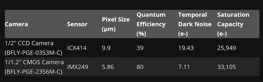
In the next figure we can see a comparison between ¼" and ½" CCD sensors.

As we can see the ½’’ sensor generates a higher signal for the same light density. We can also see that saturation happens at a similar light density level of 700 photons/µm², but the ½’’ sensor has significantly higher saturation capacity.
Next graph demonstrates that the light level at which signal is equal to the noise, known as the absolute sensitivity threshold, is reached by the ½’’ sensor at a slightly lower level than that of the ¼'’ sensor.


Based on the higher signa-to-noise ratio of the ½’’ sensor, we can assume that the ½’’ cameras perform better than ¼’’ cameras at low light levels. Which tells us that sensor size is something we shouldn't neglect.
Measurements above being made with CCD sensors doesn't mean that same principle can't be applied to CMOS as well. We can even compare smaller CCD to a bigger CMOS.
Going back to the nature of the theme of this article - an APS-C sensor found in mentioned Pentax camera is twice the size of an IMX989, so overall it generates higher signal and has higher well capacity as well.

Sensor size defferences and their noise characteristics examples are nicely covered in this video.
Pixel size and noise
The next issue is the physical pixel pitch. Problem is that well capacity declines with smaller pixel size. This has consequences both for high and low levels of scene luminance and for short and long exposure durations. Small pixels simply have fewer photons incident at their aperture than large pixels and saturate at lower photometric exposure values. These properties have implications for sensor dynamic range and signal-to-noise ratios.

Figure 1 plots the sensor SNR for color imaging sensors with pixels described in Table 1. The peak SNR declines with pixel size mainly because well-capacity (maximum number of electrons prior to saturation) decreases with pixel size from about 37,500 (5.2µm) to 16,000 (2µm) electrons. The reduction in well-capacity alone, without any other noise contributions, would produce a decline in the peak SNR of more than 3dB. The SNR drop is larger, however, because the effect of noise is more significant when added into lower signal levels. Thus, even though the technology advances in lower levels of read noise and dark voltage, their impact remains high because these noises are superimposed on relatively low signal levels. The peak SNR of the smallest pixel is approximately 8dB lower than that of the largest pixel.

In smartphone imaging manufacturers are coming with smaller and smaller pixel sizes, so they have to come up with more and more tricks to overcome SNR declines. One of the ways is to go higher resolutions. There is a simple way to make noise measurements independent from the pixel count: we can normalize the noise for a given sensor resolution. For instance, a 16Mpix sensor can be transformed into an 8Mpix sensor by averaging pixels by pairs (binning), resulting in a twice smaller noise variance. More generally, for a sensor with N Mpix, we multiply the noise variance by a factor 8/N. With this normalization, SNR essentially depends on the sensor size, when photon shot noise dominates. Doubling the pixel count of a sensor introduces a correction offset of 3dB. However higher pixel count itself results in even smaller pixel pitches - more pixels means smaller pixels, less light on each pixel and eventually a lower signal to noise ratio.
Binning issues
Binning is the same as adding the charge of 2 or more pixels together. The charge in the target pixel then represents the illumination of 2 (or more) pixels. It is possible to bin pixels vertically by shifting two image rows into the horizontal register without reading it after the first shift. It is also possible to bin pixels horizontally by shifting the horizontal register two times into output node without resetting it after the first shift. Horizontal binning cannot be done on the image sensor; this is done in the digital domain in the image processing. Vertical binning, however, can be done on the sensor level. With vertical binning, the charge of multiple lines is combined before they are readout. For binning of 4 lines this means vertical transport of 4 lines and after that the horizontal transport of this binned line takes place. After that the cycle of vertical transport of 4 lines and horizontal readout starts again. Combining of both vertical and horizontal binning leads to square (or rectangular) image binning. For example 2×2 binning is a combination of 2× vertical and 2× horizontal binning.
Owing to the fact that the image sensor resolution exceeds the optical resolution in many applications, binning is an attractive way to trade off the excess spatial resolution for gains in SNR. The only problem being that electrical charge of several adjacent binned to 3.2μm pitch pixels does not equal that of a physical sized actual 3.2μm pixel. You mostly overcome small pixels quantum efficiency issues at this point, hardly reaching levels of a non-binned larger size pixel. Not to mention the process of binning not being fully hardware might lead to certain losses of data while processing, as well as introducing demosaic/remosaic challenges for overall image quality.
Miniature pixels crosstalk issues
Besides pervious information we have to take into account so-called crosstalk problems while comparing large sensors with large pixels and smaller sensors with smaller pixels binned to improve QE. Crosstalk is a parasitic charge exchange between neighboring pixels. So when doing binning - you're doing it upon bloated by crosstalk data.

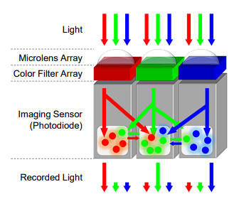
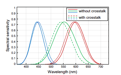
There are several crosstalks - optical, spectral and electrical. All affect degradation of quality but I would like to more focus on electrical one. Electrical crosstalk consists in the diffusion of electrical charge (electrons or holes depending the pixel type) between adjacent pixels. It occurs in silicon material due to electrical mechanisms (diffusion and drift). Crosstalk occurs when photons falling on one pixel are “falsely” sensed by other pixels around it. For example, we call it crosstalk if we shine highly focused light only on a red pixel, and the nearby blue pixel shows a response.

In this extreme case, the blue channel response will be too high and skew the real pixel color. Reducing crosstalk in small pixels has thus become one of the most difficult and time-consuming tasks in sensor design. This doesn’t mean that a bigger sensor with larger pitch is not affected by crosstalk at all - crosstalk is a universal issue in CMOS sensors. But the problem hits harder the smaller pixel size we go - as the smaller the pixel is, the more interfered signals it gets coming its neighbors. Manufacturers have to come up with better isolation between pixels which becomes a challenge for high resolution (high megapixel count) miniature pixel sensor designs.
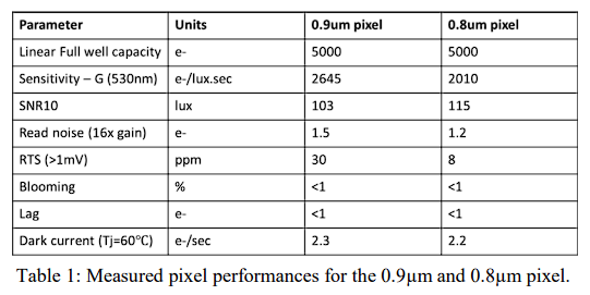
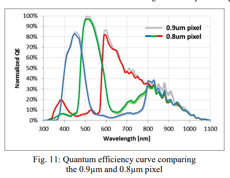
For example OmniVision was capable of improving its results coming from 0.9µm to 0.8µm by effectively utilizing backside deep trench isolation novelties to overcome electrical crosstalk. However even as small as 0.1µm shrinkage in pixel size resulted in near 24% drop of sensitivity. As we learned already this gap will only get bigger when we compare 0.8µm with monstrous 3.7µm that is more than 4x bigger, so its sensitivity efficiency would be around 96% greater.
Conclusion
Aforementioned information does not only apply to comparison mobile sensors with its bigger brothers from a professional field - same principals apply to all classes of digital image sensors (CMOS or CCD). The key factor however remains the size - both sensor and pixel sizes equally matter for great SNR, especially on smartphones where minituarization throws in extra challanges that affect the result unless solved. Although oranges and lemons are both citrus - you better learn which used per which cocktail.
P.S #1
Regarding im989 noise "issue" with raw I can only assume 2 possible ways:
1) Xiaomi haven't fully figured out software yet - we already saw overall improvements in previous gen mi11ultra flagship last year when they dropped "dxo firmware update". It is possible that current mi12S ultra that released just yet might have its own fixes coming.
2) Xiaomi could have been very nice and despite samsung and apple attempts with expertraw & proraw - they had brains to not add excessive denoising for RAW, as that breaks the definition of raw.
Either way, any smartphone is performing denoise on various stages - first there are on-sensor corrections that result in slight denoise, then the ISP (image signal processor) performs its denoise that may vary on OEM tuning, finally it gets into software application that may denoise even further. It's likely Xiaomi would do something about it in upcoming updates and I don't think its good. If they "didn't forget" to turn the denoise this time this article probably would never come out.
P.S #2
Though there are not very much comparisons for Pentax k3 mk3 with something else of its class (i.e photocamera), there is a video where its compared against FullFrame Sony α7 III. In this given comparison a smaller sized and smaller pixel pitch pentax holds really well against bigger sized crazy 6.0µm pitch Sony.
written by UltraM8 for TechKush & Android Camera Pub
__________________
Literature:
https://corp.dxomark.com/wp-content/uploads/2017/11/2012-Film_vs_Digital_final_copyright.pdf
https://web.stanford.edu/~jefarrel/Publications/2000s/2006_Farrell_Feng_Kavusi_SPIE06_final.pdf
https://www.imagesensors.org/Past%20Workshops/2019%20Workshop/2019%20Papers/R02.pdf
https://www.jstage.jst.go.jp/article/mta/6/3/6_180/_pdf/-char/en
https://oatao.univ-toulouse.fr/302/1/estribeau_302.pdf