Via Hole

👉🏻👉🏻👉🏻 ALL INFORMATION CLICK HERE 👈🏻👈🏻👈🏻
https://computer_en_ru.academic.ru/46436/via(-hole)
переходное отверстие; межслойное отверстие (в многослойных печатных платах) fixed via free via programmable via
https://www.eurocircuits.com/via-via-hole
Перевести · A via consists of: Barrel — conductive tube filling the drilled hole Pad — connects each end of the barrel to the component, plane or trace Antipad — clearance hole between barrel and no-connect metal layer
FAQ about PCBs – What type of via hole plugging is recommended?
YouTube › Jackson Hole Mountain Resort
Blind Via Hole Examination - How to Do it!
Influence of Through Hole Vias on PCB RF Performance
NCAB Group Production process step 14: The via hole plugging process
https://cml-globalsolutions.com/wp-content/uploads/2018/03/4.Via-holes.pdf
04.03.2018 · Prior to discussing the different via protection methods, we must define “via”. It is a plated through hole with no component soldered into it and usually a diameter of …
https://www.eurocircuits.de/via-via-hole
Перевести · VIA – Via Hole. A VIA hole in a PCB consists of two pads in corresponding positions on different layers of the board, that are electrically connected by a hole through the board. The hole is made conductive by electroplating. A via …
https://www.seeedstudio.com/blog/2017/03/29/pcb-via
Перевести · 29.03.2017 · Buried Via Hole (BVH) Buried via hole connects to any circuit layer of PCB but do not pass to the outer layer. This process cannot be done using the method of bonding after drilling, it must be in the individual circuit layer when the implementation of drilling, the first part of the internal bonding after the first plating treatment, and finally all the bonding. Buried via hold need more time than the original “through-hole” and “Blind hole”, so its’ price also the most ...
https://en.m.wikipedia.org/wiki/Via_(electronics)
Ориентировочное время чтения: 5 мин
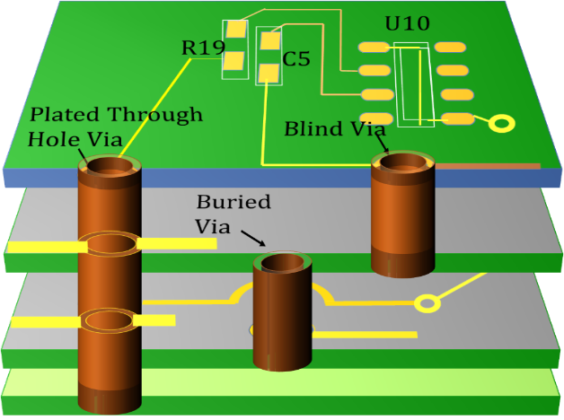
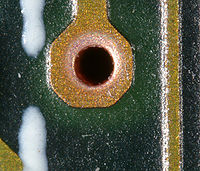
In printed circuit board (PCB) design, a via consists of two pads in corresponding positions on different layers of the board, that are electrically connected by a hole through the board. The hole is made conductive by electroplating, or is lined with a tube or a rivet. High-density multilayer PCBs may have microvias: blind vias are exposed only on one side of the board, while buried vias connect internal layers without being exposed on eith…
In printed circuit board (PCB) design, a via consists of two pads in corresponding positions on different layers of the board, that are electrically connected by a hole through the board. The hole is made conductive by electroplating, or is lined with a tube or a rivet. High-density multilayer PCBs may have microvias: blind vias are exposed only on one side of the board, while buried vias connect internal layers without being exposed on either surface. Thermal vias carry heat away from power devices and are typically used in arrays of about a dozen.
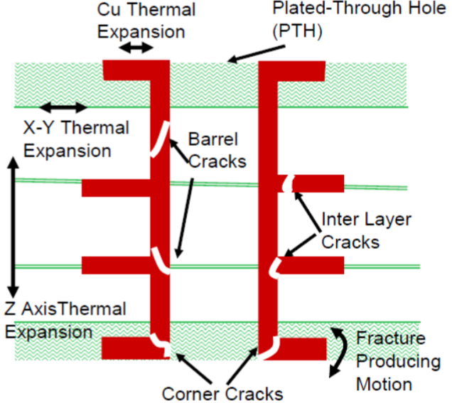
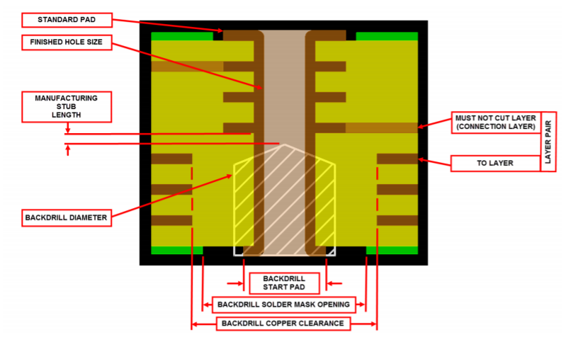
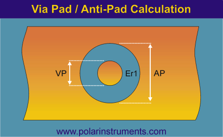
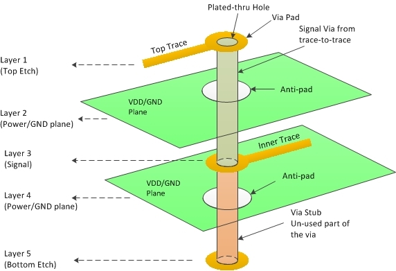
A via consists of:
1. Barrel — conductive tube filling the drilled hole
2. Pad — connects each end of the barrel to the component, plane, or trace
3. Antipad — clearance hole between barrel and metal layer to which it is not connected
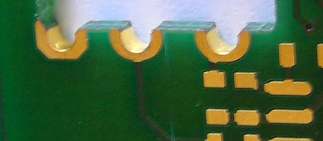
A via may be at the edge of the board so that it is cut in half when the board is separated; this is known as a castellated hole and is used for a variety of reasons, including allowing one PCB to be soldered to another in a stack.
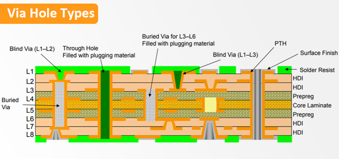
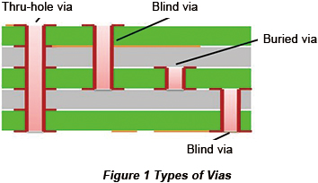
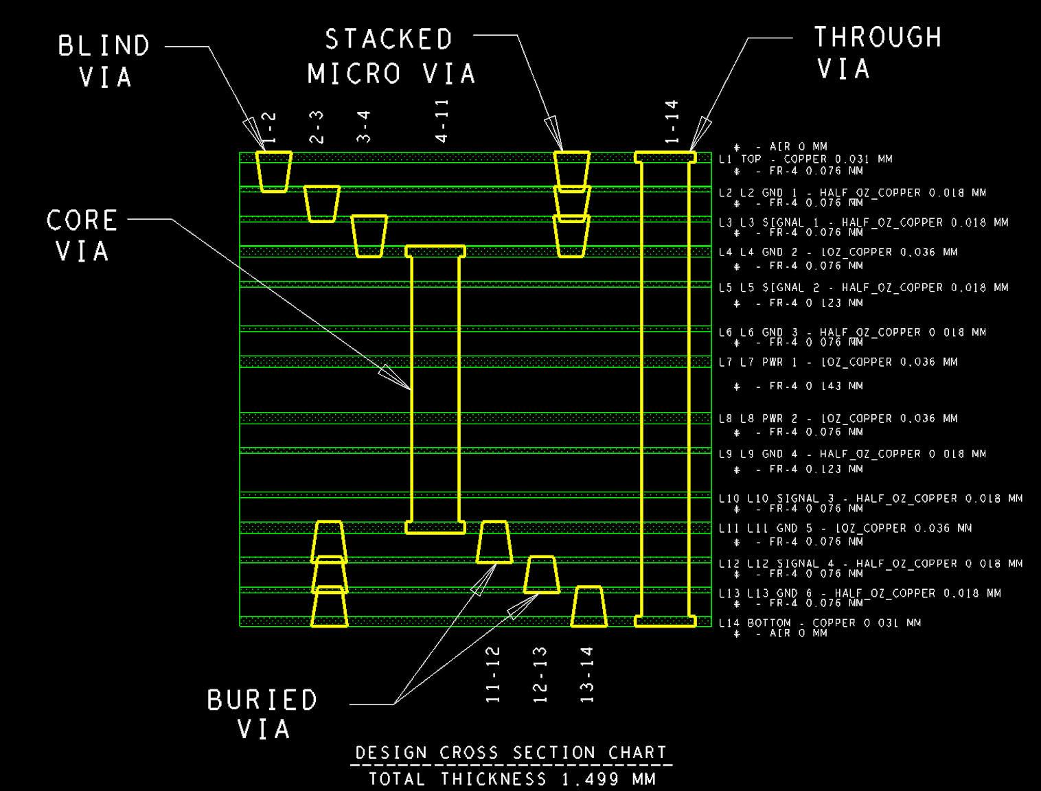
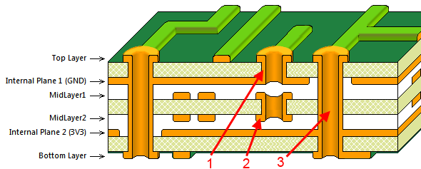
Three major kinds of vias are shown in right figure. The basic steps of making a PCB are: making the substrate material and stacking it in layers; through-drilling of plating the vias; and copper trace patterning using photolithography and etching. With this standard procedure, possible via configurations are limited to through-holes. Depth-controlled drilling techniques such as using lasers can allow for more varied via types. (Laser drills can also be used for smaller and more precisely positioned holes than mechanical drills produce.) PCB manufacturing typically starts with a so-called core, a basic double-sided PCB. Layers beyond the first two are stacked from this basic building block. If two more layers are consecutively stacked from bottom of core, you can have a 1-2 via, a 1-3 via and a through hole. Each type of via is made by drilling at each stacking stage. If one layer is stacked on top of the core and other is stacked from the bottom, the possible via configurations are 1-3, 2-3 and through hole. The user must gather information about the PCB manufacturer's allowed methods of stacking and possible vias. For cheaper boards, only through holes are made and antipad (or clearance) is placed on layers which are supposed not to be contacted to vias.
https://www.pcbdirectory.com/community/what-is-a-through-hole-via
Перевести · A Through-Hole Via is the most common type of via used in PCBs. They are formed by drilling a hole through the Printed Circuit Board from top to bottom connecting all the layers of a Multi-Layer PCB. Through hole …
A VIA hole in a PCB consists of two pads in corresponding positions on different layers of the board, that are electrically connected by a hole through the board. The hole is made conductive by electroplating.
Buried via hole connects to any circuit layer of PCB but do not pass to the outer layer. This process cannot be done using the method of bonding after drilling, it must be in the individual circuit layer when the implementation of drilling, the first part of the internal bonding after the first plating treatment,...
www.seeedstudio.com/blog/2017/03/29/pc…
What is a complete closed via hole?
What is a complete closed via hole?
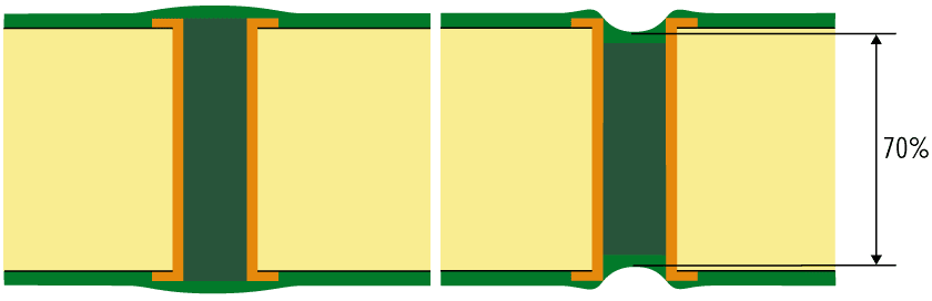
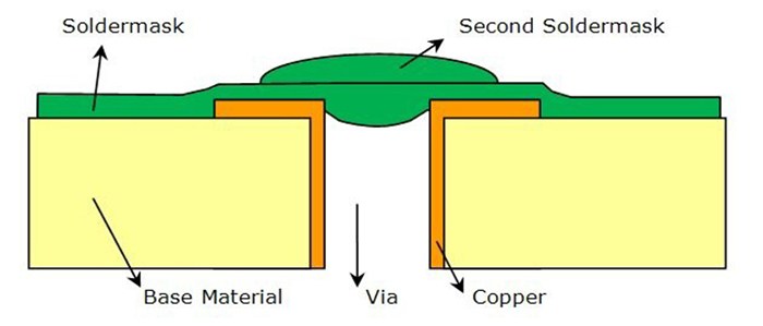
Completely closed via holes can only be guaranteed by using Via Filling. We can produce 2 types of Via Filling: Via Filling with soldermask. The vias to be filled are filled with a special hole plugging resin, TAIYO THP-100 DX1 thermally curable permanent hole filling material, using a dedicated machine, ITC THP 30 .
Is there via filling for via in pad?
Is there via filling for via in pad?
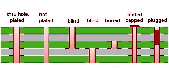
Note: This Via Filling with Resin type is suitable for Via-in-Pad application. ONLY PTH holes (PTH hole = hole with copper pad on TOP and BOT side). ONLY through hole vias, so Blind vias can NOT have Via Filling.
https://m.youtube.com/watch?v=fDY_kTLc9ik
Перевести · 21.09.2017 · Defines holes and vias, and demonstrates how to add mounting holes to …
Не удается получить доступ к вашему текущему расположению. Для получения лучших результатов предоставьте Bing доступ к данным о расположении или введите расположение.
Не удается получить доступ к расположению вашего устройства. Для получения лучших результатов введите расположение.
https://computer_en_ru.academic.ru/46436/via(-hole)
переходное отверстие; межслойное отверстие (в многослойных печатных платах) fixed via free via programmable via
https://www.eurocircuits.com/via-via-hole
Перевести · A via consists of: Barrel — conductive tube filling the drilled hole Pad — connects each end of the barrel to the component, plane or trace Antipad — clearance hole between barrel and no-connect metal layer
FAQ about PCBs – What type of via hole plugging is recommended?
YouTube › Jackson Hole Mountain Resort
Blind Via Hole Examination - How to Do it!
Influence of Through Hole Vias on PCB RF Performance
NCAB Group Production process step 14: The via hole plugging process
https://cml-globalsolutions.com/wp-content/uploads/2018/03/4.Via-holes.pdf
04.03.2018 · Prior to discussing the different via protection methods, we must define “via”. It is a plated through hole with no component soldered into it and usually a diameter of …
https://www.eurocircuits.de/via-via-hole
Перевести · VIA – Via Hole. A VIA hole in a PCB consists of two pads in corresponding positions on different layers of the board, that are electrically connected by a hole through the board. The hole is made conductive by electroplating. A via …
https://www.seeedstudio.com/blog/2017/03/29/pcb-via
Перевести · 29.03.2017 · Buried Via Hole (BVH) Buried via hole connects to any circuit layer of PCB but do not pass to the outer layer. This process cannot be done using the method of bonding after drilling, it must be in the individual circuit layer when the implementation of drilling, the first part of the internal bonding after the first plating treatment, and finally all the bonding. Buried via hold need more time than the original “through-hole” and “Blind hole”, so its’ price also the most ...
https://en.m.wikipedia.org/wiki/Via_(electronics)
Ориентировочное время чтения: 5 мин
In printed circuit board (PCB) design, a via consists of two pads in corresponding positions on different layers of the board, that are electrically connected by a hole through the board. The hole is made conductive by electroplating, or is lined with a tube or a rivet. High-density multilayer PCBs may have microvias: blind vias are exposed only on one side of the board, while buried vias connect internal layers without being exposed on eith…
In printed circuit board (PCB) design, a via consists of two pads in corresponding positions on different layers of the board, that are electrically connected by a hole through the board. The hole is made conductive by electroplating, or is lined with a tube or a rivet. High-density multilayer PCBs may have microvias: blind vias are exposed only on one side of the board, while buried vias connect internal layers without being exposed on either surface. Thermal vias carry heat away from power devices and are typically used in arrays of about a dozen.
A via consists of:
1. Barrel — conductive tube filling the drilled hole
2. Pad — connects each end of the barrel to the component, plane, or trace
3. Antipad — clearance hole between barrel and metal layer to which it is not connected
A via may be at the edge of the board so that it is cut in half when the board is separated; this is known as a castellated hole and is used for a variety of reasons, including allowing one PCB to be soldered to another in a stack.
Three major kinds of vias are shown in right figure. The basic steps of making a PCB are: making the substrate material and stacking it in layers; through-drilling of plating the vias; and copper trace patterning using photolithography and etching. With this standard procedure, possible via configurations are limited to through-holes. Depth-controlled drilling techniques such as using lasers can allow for more varied via types. (Laser drills can also be used for smaller and more precisely positioned holes than mechanical drills produce.) PCB manufacturing typically starts with a so-called core, a basic double-sided PCB. Layers beyond the first two are stacked from this basic building block. If two more layers are consecutively stacked from bottom of core, you can have a 1-2 via, a 1-3 via and a through hole. Each type of via is made by drilling at each stacking stage. If one layer is stacked on top of the core and other is stacked from the bottom, the possible via configurations are 1-3, 2-3 and through hole. The user must gather information about the PCB manufacturer's allowed methods of stacking and possible vias. For cheaper boards, only through holes are made and antipad (or clearance) is placed on layers which are supposed not to be contacted to vias.
https://www.pcbdirectory.com/community/what-is-a-through-hole-via
Перевести · A Through-Hole Via is the most common type of via used in PCBs. They are formed by drilling a hole through the Printed Circuit Board from top to bottom connecting all the layers of a Multi-Layer PCB. Through hole …
A VIA hole in a PCB consists of two pads in corresponding positions on different layers of the board, that are electrically connected by a hole through the board. The hole is made conductive by electroplating.
Buried via hole connects to any circuit layer of PCB but do not pass to the outer layer. This process cannot be done using the method of bonding after drilling, it must be in the individual circuit layer when the implementation of drilling, the first part of the internal bonding after the first plating treatment,...
www.seeedstudio.com/blog/2017/03/29/pc…
What is a complete closed via hole?
What is a complete closed via hole?
Completely closed via holes can only be guaranteed by using Via Filling. We can produce 2 types of Via Filling: Via Filling with soldermask. The vias to be filled are filled with a special hole plugging resin, TAIYO THP-100 DX1 thermally curable permanent hole filling material, using a dedicated machine, ITC THP 30 .
Is there via filling for via in pad?
Is there via filling for via in pad?
Note: This Via Filling with Resin type is suitable for Via-in-Pad application. ONLY PTH holes (PTH hole = hole with copper pad on TOP and BOT side). ONLY through hole vias, so Blind vias can NOT have Via Filling.
https://m.youtube.com/watch?v=fDY_kTLc9ik
Перевести · 21.09.2017 · Defines holes and vias, and demonstrates how to add mounting holes to …
Не удается получить доступ к вашему текущему расположению. Для получения лучших результатов предоставьте Bing доступ к данным о расположении или введите расположение.
Не удается получить доступ к расположению вашего устройства. Для получения лучших результатов введите расположение.
Black Hole Sabotage 2021
Sexy Girls In Higher Heels
Ftv Girls Upskirt No Panties
Hair Job Porno
Worm Hole
via(-hole) - это... Что такое via(-hole)?
VIA HOLES – MANY WAYS TO CLOSE THEM
VIA - Via Hole - Eurocircuits
Via Hole