The CCD - FLI Camera PDFs
 CCD vs CMOS Sensors - YouTube
The Single Strategy To Use For CCD detectors in high-resolution biological electron microscopy
A one-dimensional selection, used in line-scan electronic cameras, records a single slice of the image, whereas a two-dimensional range, used in video and still video cameras, catches a two-dimensional image corresponding to the scene predicted onto the focal airplane of the sensor. When the variety has been exposed to the image, a control circuit triggers each capacitor to move its contents to its next-door neighbor (operating as a shift register).
By duplicating this procedure, the controlling circuit converts the whole contents of the array in the semiconductor to a series of voltages. In a digital device, these voltages are then sampled, digitized, and typically kept in memory; in an analog device (such as an analog camera), they are processed into a constant analog signal (e.
by feeding the output of the charge amplifier into a low-pass filter), which is then processed and fed out to other circuits for transmission, recording, or other processing. Detailed physics of operation [modify] Charge generation [modify] Before the MOS capacitors are exposed to light, they are prejudiced into the deficiency area; in n-channel CCDs, the silicon under the bias gate is a little p-doped or intrinsic.
However, it requires time to reach this thermal equilibrium: approximately hours in high-end scientific video cameras cooled at low temperature level. Initially after biasing, the holes are pressed far into the substrate, and no mobile electrons are at or near the surface area; the CCD hence operates in a non-equilibrium state called deep deficiency.
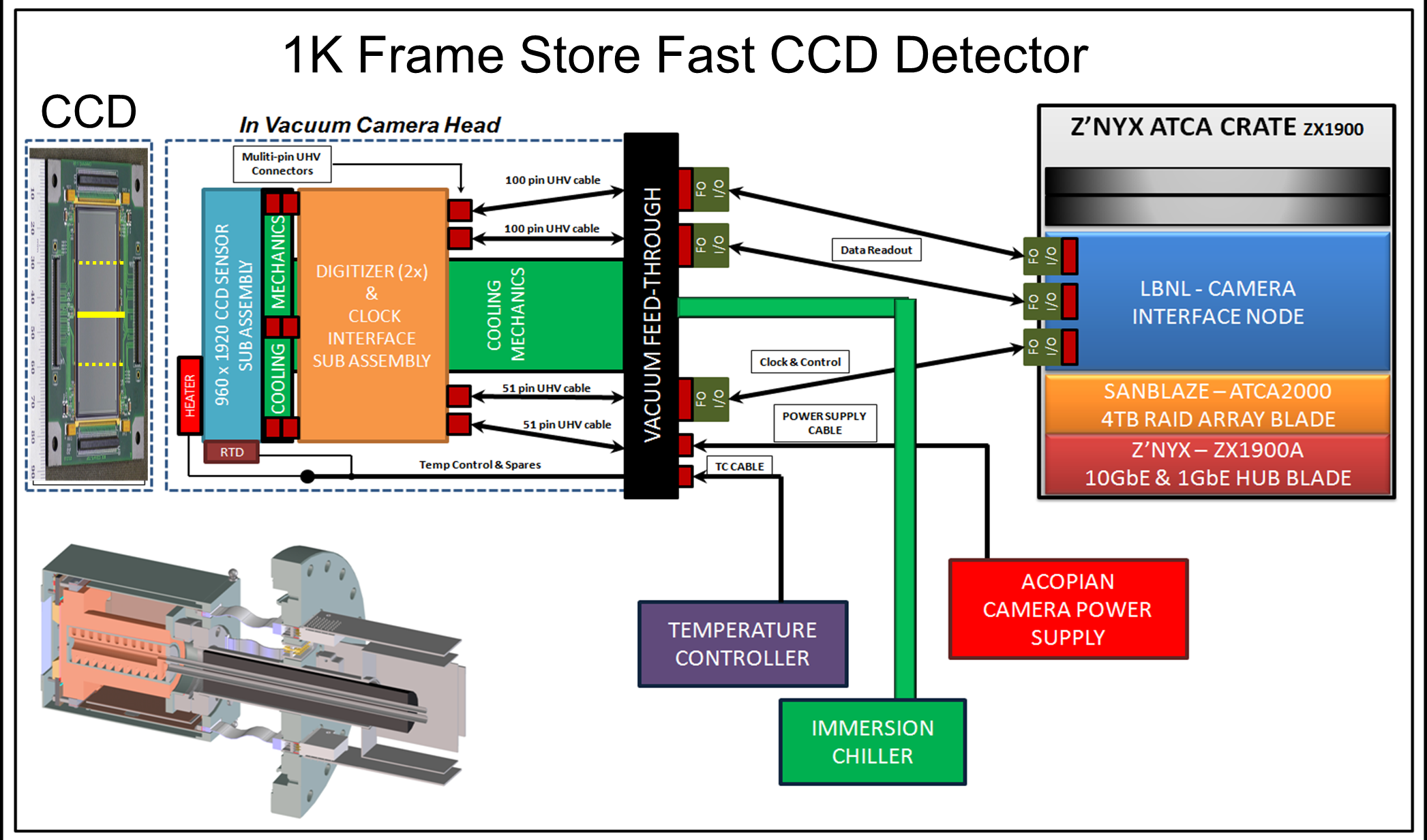
Facts About new CCD detector for the Virtual Telescope Project - Indiegogo Uncovered
4 pair-generation processes can be recognized: photo-generation (approximately 95% of quantum efficiency), generation in the exhaustion region, generation at the surface, and generation in the neutral bulk. The last 3 processes are referred to as dark-current generation, and add noise to the image; they can limit the total functional combination time.
In this case, the well is stated to be full. Check it Out of each well is referred to as the well depth, usually about 105 electrons per pixel. Style and production [modify] The photoactive area of a CCD is, usually, an epitaxial layer of silicon. It is lightly p doped (normally with boron) and is grown upon a substrate material, often p++.