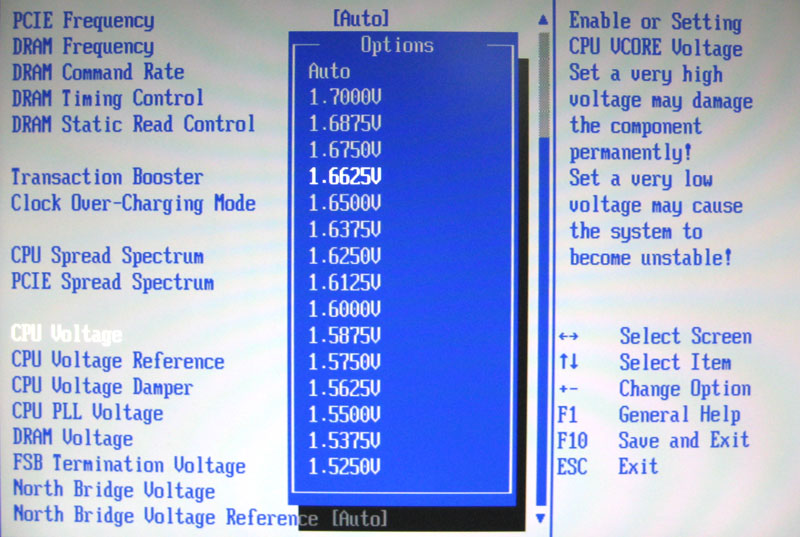
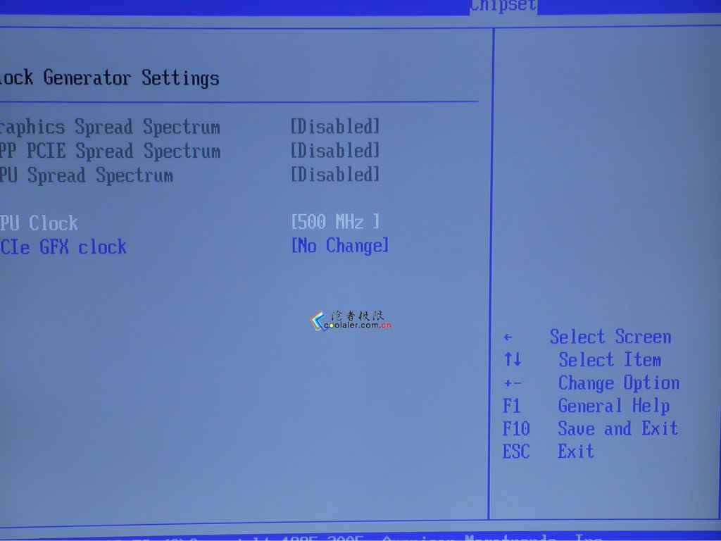
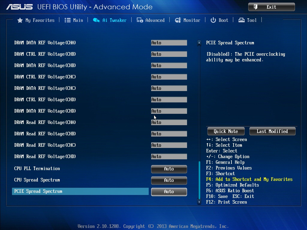
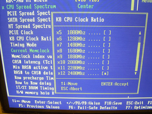
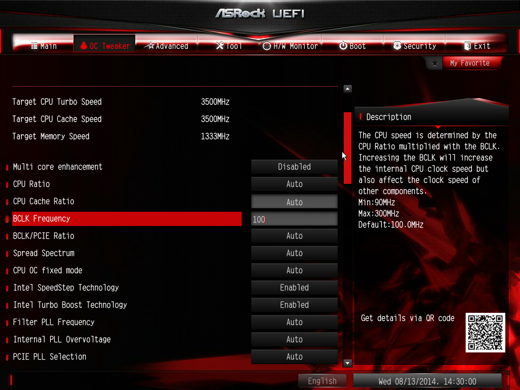
Pcie Spread Spectrum

🔞 ALL INFORMATION CLICK HERE 👈🏻👈🏻👈🏻
Pcie Spread Spectrum
© 2008—2012, Александр Микляев. Все материалы, находящиеся на этом сайте, являются авторскими и защищены российским и международным законодательствами. Использование их в сетевых и офлайновых изданиях без письменного разрешения автора не допускается. Наличие ссылки на оригинал не является оправданием для кражи. Вы можете цитировать описания отдельных опций в частной переписке, при обсуждениях на интернет-форумах, досках объявлений, при написании комментариев к другим статьям при условии наличия рядом с цитатой ссылки на этот сайт. Если вам понравился ресурс, информация, приведенная здесь, помогла в решении ваших проблем с компьютером, буду благодарен за размещение ссылки на данный сайт.
Rampage IV Extreme UEFI BIOS Guide For Overclocking | ROG - Republic of...
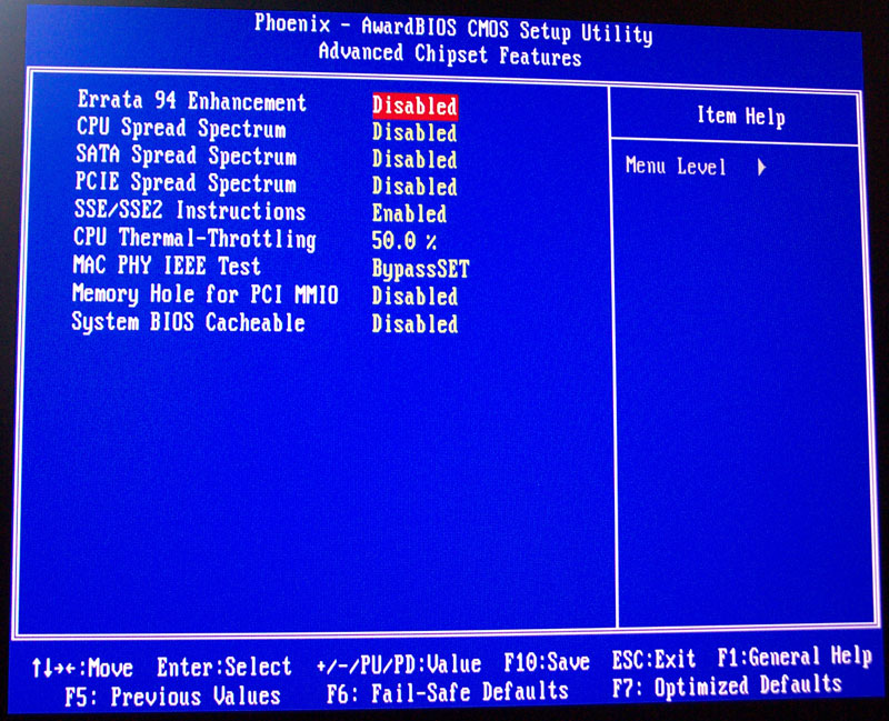
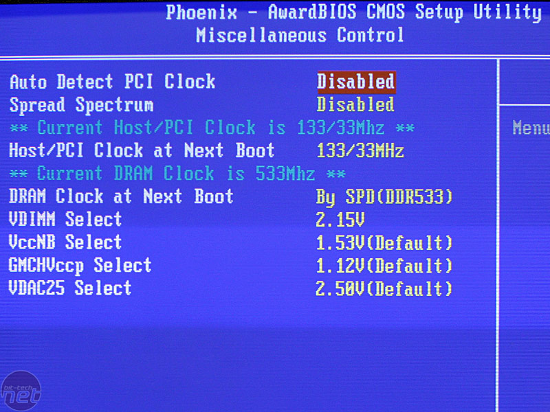
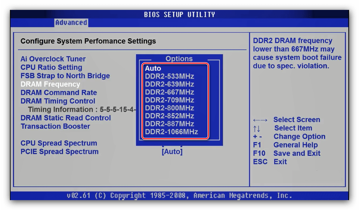
Настройка BIOS :: Алфавитный список всех опций
PCIe Spread Spectrum Clocking (SSC) for Verification Engineers | Synopsys
Spread - spectrum clocking in PCI Express - EDN
Spread spectrum - Wikipedia
This post is filed under Methodology , PCIe .
5G
AI
Arm
Automotive
CAN
Ethernet AVB
FlexRay
LIN
CCIX
CXL
Data Center
Ethernet
HBM
HMC
PCIe
Debug
DesignWare
events
FlexE
IoT
JESD
Methodology
UVM
Mobile SoC
Interface Subsystems
Audio
I2S
SlimBus
Soundwire
Camera
C-PHY
CSI
D-PHY
MPHY
Unipro
Display
DisplayPort
DSC
DSI
HDCP
HDMI
MHL
eMMC
I3C
ONFi
UFS
USB
MIPI
Processor Subsystems
AMBA
ACE
AXI
CXS
Interconnects
CCI400
CHI
NOC
Memory
DDR
DFI
Flash
SPI
ToggleNAND
LPDDR
Type C
Storage
FC
NVMe
SAS
SATA
Success Stories
SystemVerilog
Test Suites
Uncategorized
Products
Software Integrity
Semiconductor IP
Verification
Design
Silicon Engineering
Resources
Solutions
Services
Support
Community
Manage Subscriptions
Corporate
About Us
Careers
Corporate Social Responsibility
Investor Relations
Contact Us
Legal
Privacy
Trademarks & Brands
Software Integrity Agreements
©2021 Synopsys, Inc. All Rights Reserved
Posted by VIP Experts on December 15, 2015
Many of us who work primarily in digital verification and design are shielded from physical layer details. Only a handful of specialists closely follow these details. So for the rest of us, verifying and debugging Spread Spectrum Clocking (SSC) can be a daunting task.
This blog post is a quick Q&A to give you a jump start in understanding some of the complexities of PCI Express (PCIe) Spread spectrum clocking (SSC) techniques.
Here’s where you can learn more about Synopsys VC Verification IP for Gen 4 ready PCIe and PCIe Test Suites .
What is Spread Spectrum Clocking? Why is it used?
Spread spectrum clocking is the process by which the system clock is dithered in a controlled manner so as to reduce peak energy content. SSC techniques are used so as to minimize Electromagnetic Interference (EMI) and/or pass Federal Communications Commission (FCC) requirements.
If you transform a clock signal to frequency domain, you will spot a high energy spike at the frequency of clock (nonspread blue spike at 3GHz in Figure 1 below). Spread spectrum is a way to distribute this spike over a band of frequencies to reduce the power at the frequency of signal (Red-colored spread in Figure 1).
Figure 1: Spectral Amplitude Reduction of 3GHz Clock with Spread Spectrum Clocking
You can learn more about SSC from Synopsys Fellow John Stonick in this short YouTube video .
How is Spread Spectrum Clocking achieved?
Spread spectrum clocking uses modulation to achieve the spread of the spectral power. The carrier signal which is typically a high frequency clock signal is modulated with the low frequency modulator signal for frequency modulation. While the overall energy is unchanged, the peak power is reduced. The amount of peak energy dispersion is dependent on the modulation bandwidth, spreading depth and spreading profile.
The resulting SSC modulated carrier signal ends up with the much higher jitter than the unmodulated carrier signal.
The most common modulation techniques are down-spread and center-spread:
Figure 2 below shows a 3Ghz carrier clock signal, down-spread with 0.5 % using the 30KHz triangular wave. On the Y-axis, you can see the carrier frequency rise and fall. All spread carrier frequency values remain below the 3 GHz.
Figure 2: 3GHZ Carrier signal frequency variation with 0.5% Down-spread SSC clocking
What are different clocking architectures supported by PCIe? Do all of them support SSC?
There are three different types of clocking architectures supported by PCIe:
Common Refclk is the most widely supported architecture among commercially available devices. However, the same clock source must be distributed to every PCIe device while keeping the clock-to-clock skew to less than 12 ns between devices. This can be a problem with large circuit boards or when crossing a backplane connector to another circuit board.
If a low-skew configuration isn’t workable, such as in a long cable implementation, the Separate Refclk architecture, with independent clocks at each end, can be used. But Gen 2.0 base specification did not allow the SSC on the Separate Refclk implementation. It was only enabled through ECN: Separate Refclk Independent SSC (SRIS) Architecture in 2013 which became part of the 3.1 base specifications released in Nov 2013.
The Data Clocked Refclk architecture is the simplest, as it requires only one clock source, at the transmitter. The receiver extracts and syncs to the clock embedded in the transmitted data. Data-clocked architecture was introduced when the PCIe 2.0 standard was released in 2007.
You can learn more about clocking architectures here .
To learn more about SRIS, here is yet another insightful short video from Synopsys Fellow John Stonick.
Yes. All four speeds 2.5 GT/s (Gen 1), 5 GT/s (Gen 2), 8 GT/s (Gen3) and 16 GT/s (Gen4) can support SSC. Same spread spectrum clocking parameters apply for all the four speeds.
Figure 3: Snapshot of Refclk Parameters from Gen 4 PCIe Base Specification (Source: PCI-SIG)
Some key parameters we need to note in the above table:
What is the value provided by verification for spread spectrum clocking?
From a design under test (DUT) point of view, the primary value is in the verification of the receiver’s clock data recovery modeling to handle the large variation in the jitter (up to 5600 ppm) especially in the SRIS mode.
How can I visually verify if SSC is really happening?
There are multiple ways. The simplest is you can visualize the “clock period signal” typically a floating point data type (real type in SystemVerilog) if it’s accessible in your waveform viewer as analog signal.
If it’s not accessible, through a simple monitor collect the time stamp and period of the Refclk or internally generated transmit bit clock running at line speed, for at least 33us assuming you are using 30Khz modulation. Plot the timestamp on the X-axis and duration of the clock on the Y-axis. You should be able to see a profile matching the one shown in Figure 2.
In order for you to successfully verify spread spectrum clocking, the PCIe Verification IP you use needs to support SSC. It should give you the programmability to turn spread spectrum ON or OFF at different speeds. Also it should support the specification defined SSC profile for Down-spread of 0.5%. It should also allow programmability in terms of the frequency of modulated signal in the range of 30Khz (min) and 33Khz (max). Synopsys PCIe VIP comes loaded with all these features and more.
Here’s where you can learn more about Synopsys VC Verification IP for Gen 4 ready PCIe and PCIe Test Suites .
Authored by Narasimha Babu G V L , Udit Kumar and Anand Shirahatti
Videos Nasty For Erotica
Txxx Ru
Minet Oral Sex
Granny Stripping
Naughty America Nicole