How the Silicon Wafer Manufacturing Process Works
Silicon Specialist LLCIf you've been wondering how the entire Silicon Wafer Manufacturing Process works, then read this article. You'll discover the various steps involved in silicon wafer fabrication, from inspection to etching to lapping and grinding.
Once you understand the entire process, you'll be well on your way to implementing it in your own business. It's time to get started. Here are the benefits of as-cut wafers.
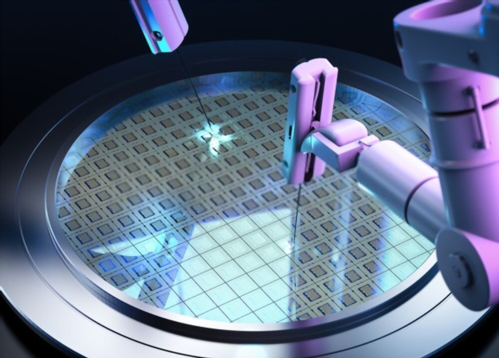
Wafer Inspection
The silicon wafer manufacturing process includes a step for detecting defects on the wafer. The defect-detecting step occurs after cleaning, drying, and packaging the wafer. The defects are identified using a microscope to detect the exact location and size of the defect. A monitoring unit, such as a CCD camera, also performs the defect-detecting step. The laser beams are then converged using the converging lens 22.
Many types of defects can occur in the silicon wafer. A conventional defect called COP cannot be detected with a dark field microscope or an atomic force microscope. The defect may also be the result of a difference in surface quality or density caused by impurities. During Wafer Inspection, experts check for these defects and ensure that the silicon is clean. Wafer defects are not considered defects if they are not visible to the naked eye, but they are still important.
Wafer Etch
The first step in the silicon wafer manufacturing process is to apply an etching solution to the silicon wafer. The etching chemicals are applied to the wafer and must be agitated so that the atoms can spread out evenly throughout the ion source. During the etching process, a qualified technician will answer any questions about the etching process. Once the etching solution is applied, the silicon wafer will be subjected to a process known as photolithography.
Once the etching is complete, the silicon wafer is ready to be placed into the machine. This step is known as the edge etching process, and the peripheral edge of the wafer is immersed in the etchant for a specific duration of time. The rotation rate is set to prevent the etchant from flowing inward and causing damage to the machine. This step is crucial in silicon wafer manufacturing because it allows the silicon wafer to maintain its ideal shape.
Wafer Lapping
Before polishing begins, the silicon workpiece is subjected to various machining processes. Wafer lapping removes saw marks and surface defects. This step also thins the wafer, relieving stress from the slicing process. This step is usually done in a clean room. Workers in this area wear cleanroom suits and use fans to remove any small particles from the surface. After lapping, the silicon wafer is ready to be etched.
Silicon wafers are usually cut in thin layers. After the first slicing, the next step in the manufacturing process is lapping. Wafer lapping removes rough impurities from the surface, creating a smooth, even surface several millimeters thick. University Wafer, Inc. provides this service for clients. Using double-sided lapping tools, the company can provide customized lapping services.
Wafer Grinding
The first step in silicon wafer manufacturing is to cut the ingot into blocks of specified diameters. The silicon peripheral is then ground to achieve the desired diameter. The process of lapping removes saw marks and surface defects from the silicon wafer and thins it as well. The next step is critical edge grinding, which rounds the edges of the silicon substrate to reduce the risk of breakage during later manufacturing processes.
Once the silicon wafer is ground, it needs to be cleaned. It is then examined under high-intensity light sources and laser scanning systems to ensure quality. After being inspected, the silicon wafer is packaged and shipped.
It is then placed inside an airtight outer and vacuum-sealed plastic bag. The entire process is complete in four hours, and a quality inspection can confirm the integrity of the product.
Wafer Polishing
The silicon wafers are cleaned and consolidated into process lots. Next, they undergo a complex polishing process that involves multiple steps. The purpose of this process is to increase the smoothness of the silicon surface, remove rough spots and make the surface more planar. The surface is especially critical for the flue-line geometries used in IC production. In some instances, Wafer Polishing can result in defects in the final product.
The next step in the silicon-wafer manufacturing process involves the application of dopants. These are elements from Groups 3 and 4 of the periodic table that modify the properties of the molten silicon. Common dopants include antimony, arsenic, and phosphorus.
These elements also enhance the gettering capabilities of silicon. These elements are added to silicon wafers during the manufacturing process to enhance their functionality. Silicon Specialist LLC takes care of silicon wafer manufacturing and provides a good quality silicon wafer to you.