FPGA & Quartus first setup guide
Dmitry Alekhine (@dmfrpro)Overview of FPGA
FPGA (Field-Programmable Gate Array) is an integrated circuit that allows the developers to design a custom digital logic in the field.
FPGA vs General-Purpose Processor (GPP)
- ✅FPGA is reprogrammable: you define your own digital logic using HDL
- ✅FPGA has changeable ISA: you define your own ISA by designing logic circuits
- ✅FPGA is faster: generic architecture of GPP leads to looses in performance in comparison with specifically optimized solutions on FPGA and HDL
- ❌FPGA is expensive: depending on model and brand, but typically GPPs are cheaper
- ❌FPGA is energy inefficient: GPPs consume less power
Overview of MAX10 and Cyclone IV E
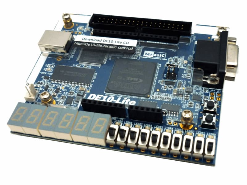
We will use the following 2 FPGA boards:
- MAX10 DE10-Lite (
10M50DAF484C7G) - Cyclone IV E A4-CE10 (
EP4CE10E22C8N)

Recommended materials
- Andrew Moore & Ron Wilson "FPGAs for dummies" - a free online book from Intel
- Intel Quartus Prime Pro and Standard Software User Guides
- DE10-Lite User Manual
- EP4CE10 User Manual
Installation process
Make sure that you have enabled CPU virtualization support. Otherwise, you will get errors during installation.

Download and install Virtualbox, Extension Pack and VM image
Windows / Linux Distributions / OSX
Extension Pack
VM image (~13GB)
Make sure the version of Extension Pack is the same as your Virtualbox
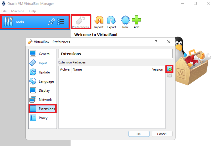
Import Extension Pack:
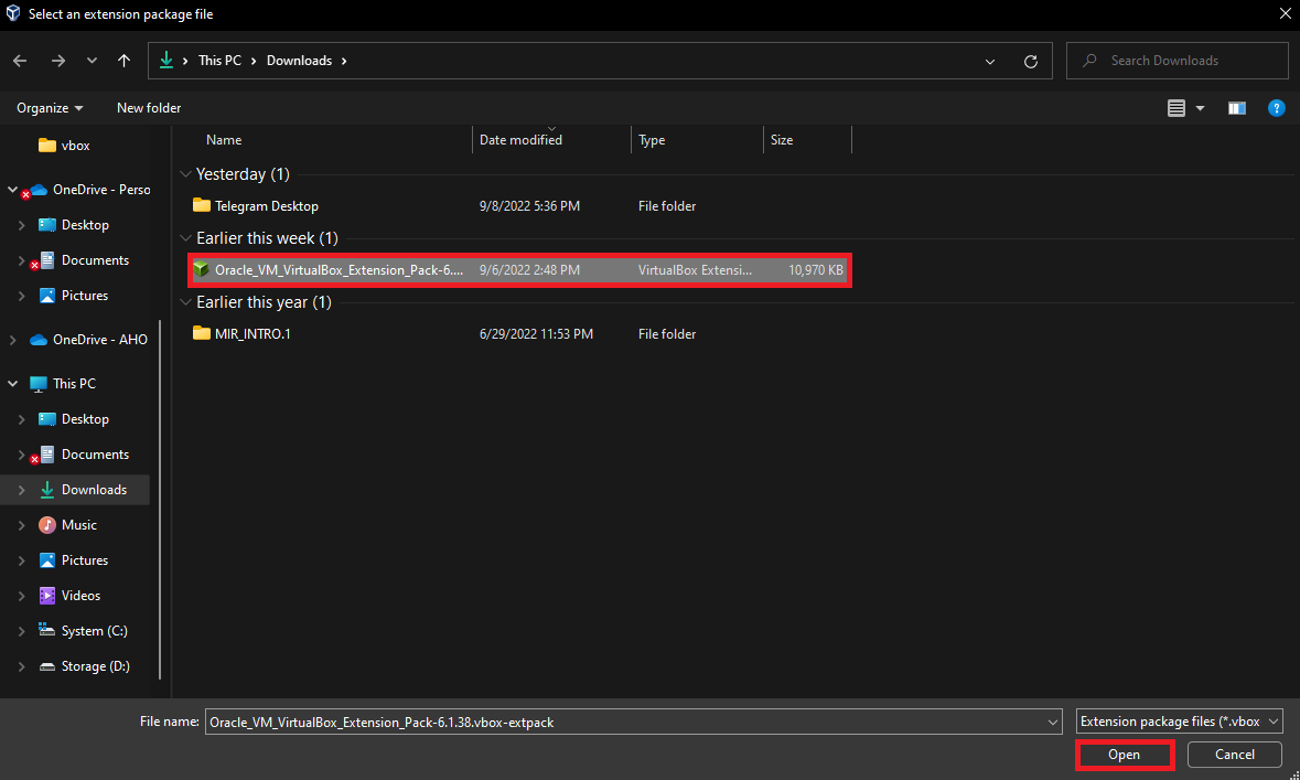
Agree with the license terms and finish the installation.
Import VM image
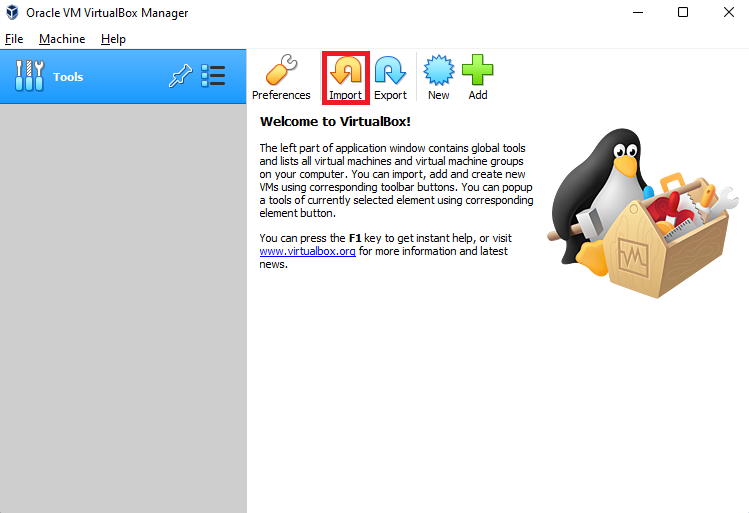
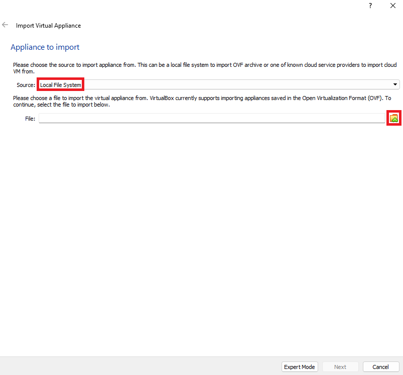
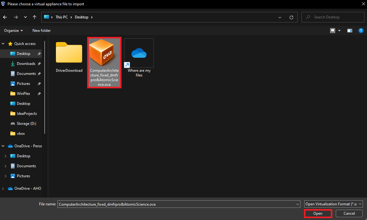
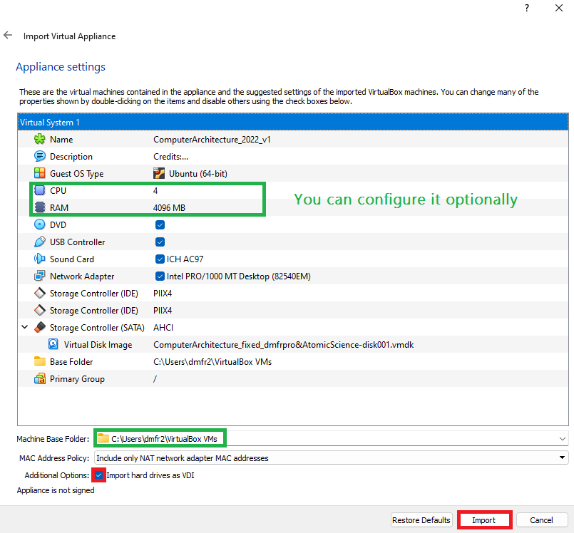
Note: If you face "Kernel Panic - not syncing: Attempted to kill the idle task!", then you must increase number os CPUs and RAM size for your virtual machine.
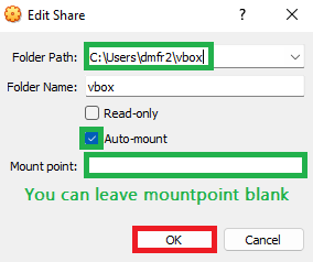
Configure shared folder
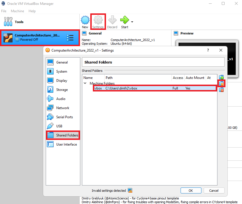
Configure USB
Now it's time to connect an FPGA device to your PC. Both Cyclone IV and MAX10 should be recognized as Altera USB-Blaster(Altera).
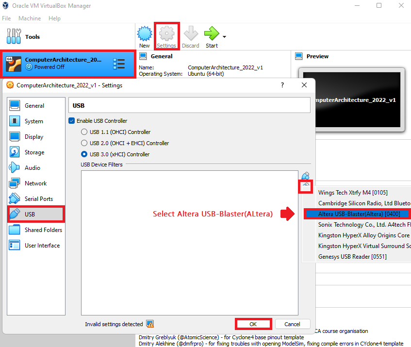
Note: If the appropriate USB device is not listed in the drop-menu, then you should try the following fixes:
Windows: Install Altera USB-Blaster drivers
Linux #1: Add the corresponding udev rules using this guide
Linux #2: Add yourself to vboxusers group by typing this command:sudo usermod -aG vboxusers your_username
You are almost there!
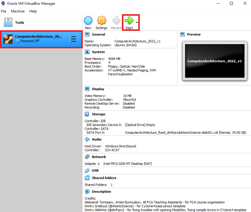
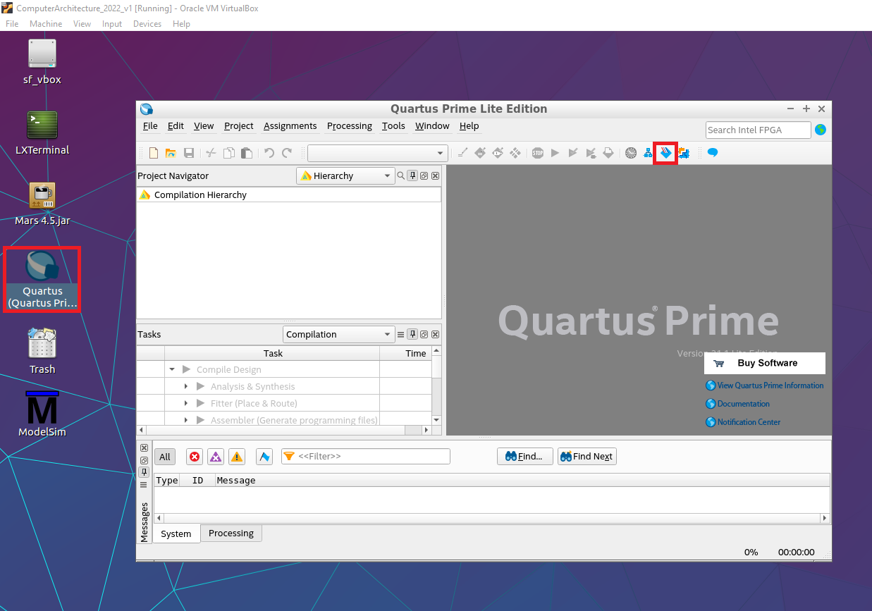
Let's start the virtual machine:
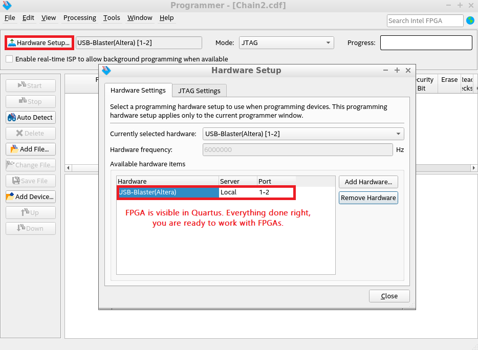
Working with FPGAs on the labs
If everything went fine, you are ready to solve the problems during the lab sessions. Let's open a prepared project:

For MAX10: /home/user/QuartusProjects/Max10/Max10.qpf
For Cyclone IV: /home/user/QuartusProjects/Cyclone4/AC4E6E10_Golden_Top.qpf
Note: both projects are based on templates. For MAX10 there exists reasy template which you can choose during new project setup. For Cyclone4 we are using a custom template which is stored in /home/user/intelFPGA_lite/templatesCreating Block Diagrams
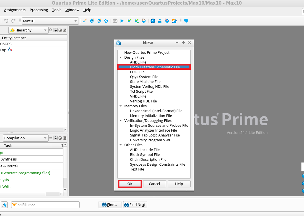
Let's create our first design. Double-click on the empty area and select a logic gate:
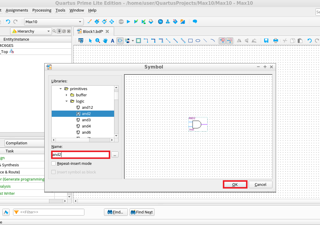
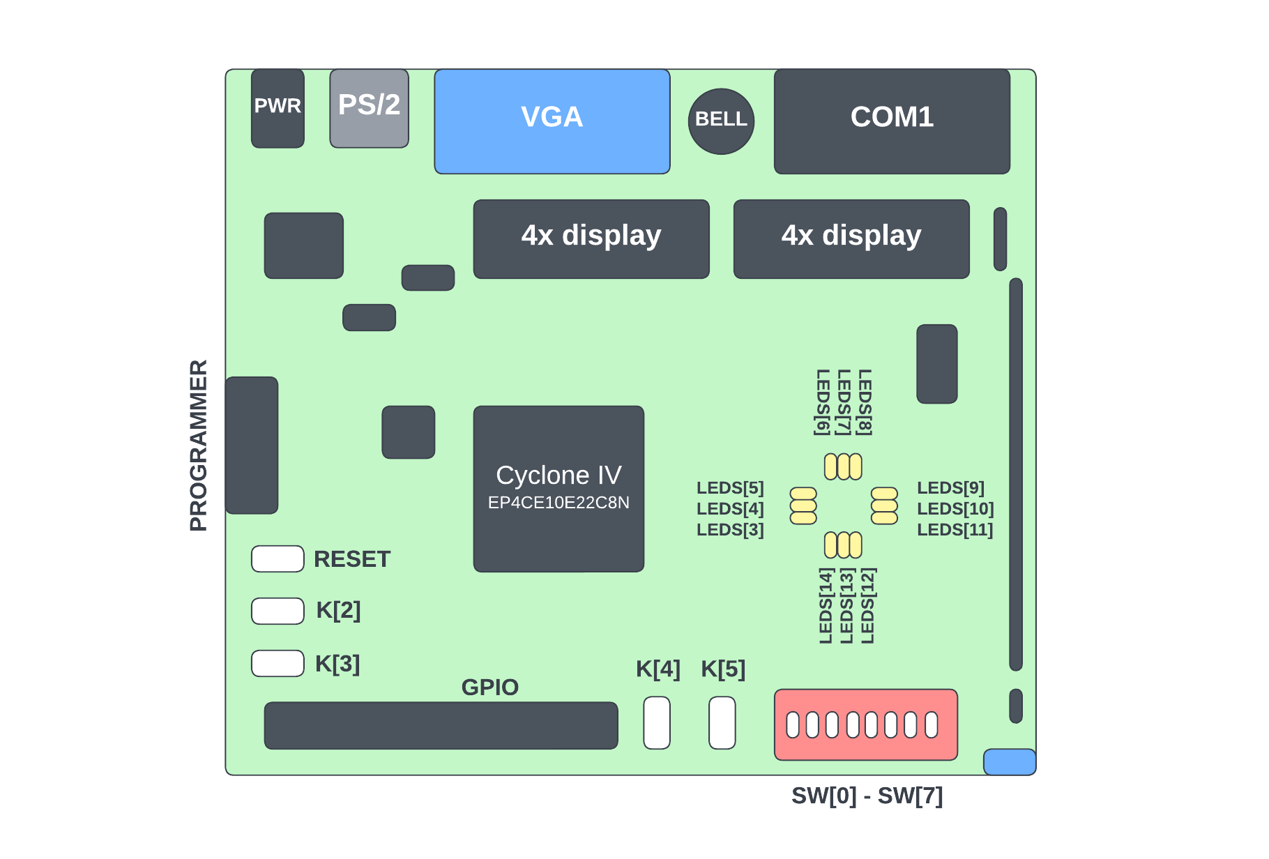
Let's add more pins and connect them. For instance, we will use input pins, and2 and output pins. On the following diagrams you can see the base pinout for switches, LEDs, and buttons:
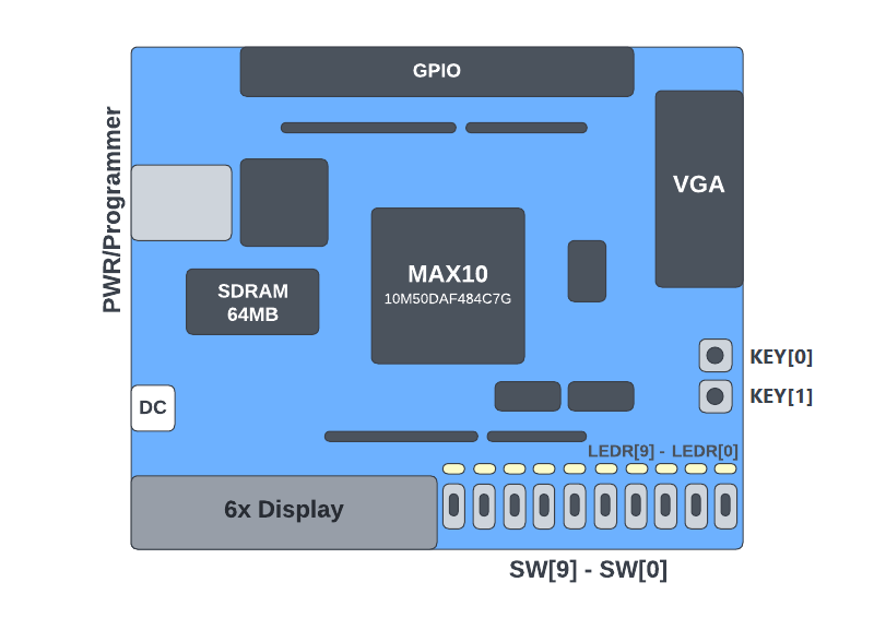
Using these diagrams, let's label our pins correctly. For instance, out input pins will be SW[0] and SW[1], and the output pin is LEDR[0]:
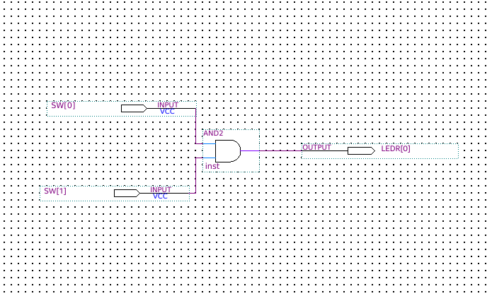
Note: on Cyclone IV all the pins have reversed behavior. You should placenotlogic gate before eachinputandoutputpin
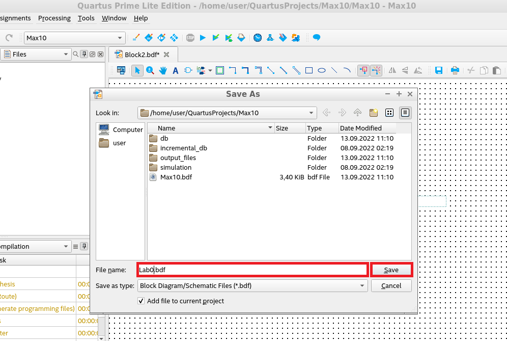
Let's save our first block diagram:
It's time to compile and flash the FPGA:
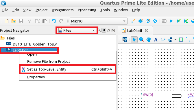
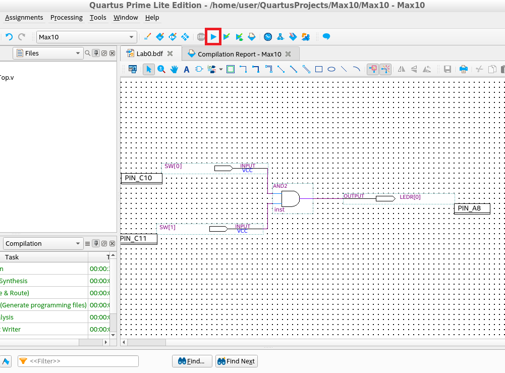
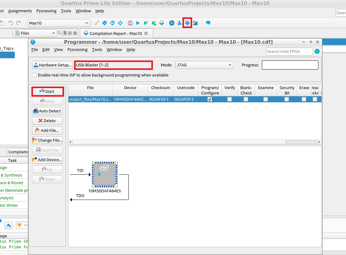
After a successful flash you can test your lab on FPGA. You can create several .bdf files, and, before flashing, set the preffered one as Top-Level Entity.
Writing verilog code
The pinout for both devices is the same as for block diagram files.
For MAX10: set DE10_LITE_Golden_Top.v as Top-Level Entity:
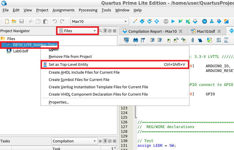
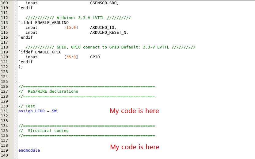
Then you can start compiltion and flash processes.
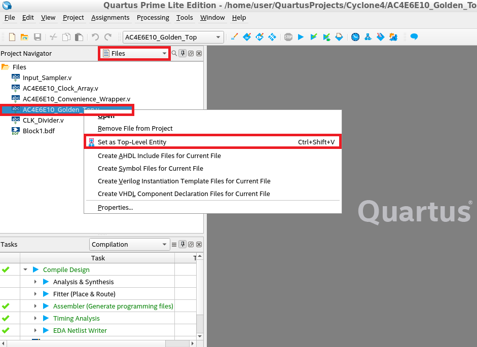
For Cyclone IV: set AC4E6E10_Golden_Top.v as Top-Level Entity:
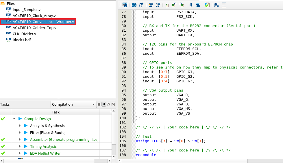
And then you must write your verilog code in AC4E6E10_Convenience_Wrapper.v:
Then you can start compiltion and flash processes.
Enabling Simulation with ModelSim
To enable device simulation, you need to perform the following steps:
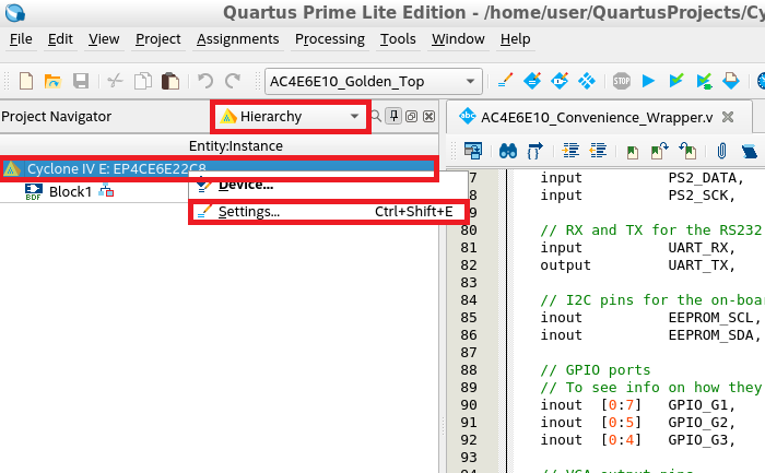

You are all set! After the compilation ModelSim will be opened, and the simulation process will begin.