Everything about the ol' Switch 2
oldpuck (with assistance from Thraktor, Look Over There, LiC, and numerous others)A number of Switch 2 technical leaks have emerged over the last few years, several of which have missed mainstream discussion. The following is a fairly complete technical summary of that information.
We'll cover The Context leading up to these discoveries, The Linux Finds that confirm many technical details of the hardware, The LinkedIn Leaks which corroborate these finds, and we will briefly summarize The NVN2 Hack and how it and the Linux finds continue to corroborate each other. Well then look at some Intriguing Reports that have come from various other sources, before summarizing What The Heck This Means
The Context
The Nintendo Switch is built around a Tegra X1 system-on-a-chip. The Tegra line is built by Nvidia, and initially struggled to find a market.
Eventually, the line split into two halves, a consumer chip and a robotics chip. The consumer line (K1, X1, X2) only found major success with the Switch. The robotics chip (Xavier) found usage in the automotive market.
The successor to Xavier is Orin, a chip which now targets the automotive market explicitly. Publicly, Nvidia has announced no new consumer Tegra.
The problem with Orin
Early speculation assumed that Orin, then, would be the basis of the next Nintendo device. Now that the chip is released, Orin itself is an extremely bad candidate
It's too big: Orin comes in three versions, Orin AGX, Orin NX and Orin Nano. Nano is the least powerful, and seems capable of powering a tablet sized device. However, the NX and the Nano are the same die as the AGX, with some parts disabled. At 455 mm², Orin is ~2.5x as big as the TX1. It simply isn't fitting into a handheld
The CPU is wrong: Orin uses an ARM A78AE CPU. The A78 is a common performance core in ARM SOCs, but the AE variant is specially built to pass new Automotive Electronics Council standards. This includes using half the cores to "safety check" the work of the other half, a huge performance and cost hit that would be inappropriate for a console
It's too rare: Nvidia hasn't disclosed the number of Orin SOCs sold, exactly, but their own marketing implies that they're selling at most a few million a year. Orin will be superseded by Nvidia Thor in 2025. Over it's lifetime, it is likely to see Wii U numbers. There simply won't be enough Orin chips made - much less binned - for Nintendo to buy.
The leak, the hack, and Nvidia's Big Mouth
June of 2021, a well known Nvidia leaker, kopite7kimi, stated that Nvidia was designing a custom chip for Nintendo called T239 (T234 is Orin)

Eight months later, Nvidia was subject to a ransomware attack. As part of that attack, the Lapsus$ group released some files. The majority of these files were unrelated to Nintendo, and included things like SSNs for employees. This was obviously awful, and I will not link to any Lapsus$ files here, only media discussion of them.
This hack included code for NVN2, a successor the NVN API that was developed by Nvidia for the original Switch. It also included T239 references, confirming the original leak.
Nvidia's big mouth
Since then, Nvidia has mentioned T239 several times in it's documentation, confirming an unannounced, consumer Tegra chip is in development.
The Linux Finds
During NX development, there were several dumps of information about the Switch that Nvidia let slip into public Linux repositories as part of it's internal development. While Nvidia has taken care to reduce those leaks this time, there are still significant finds.
The most salient point: Some of this data is from Fall 2022, some from Summer 2021, but all of it matches the NVN2 leak from Spring 2022. There is a consistent picture of the chip presented here, and as you can see elsewhere in this document, there is strong reason to believe the chip's design was finalized in Summer of 2022.
Linux 4 Tegra
Nvidia develops a Linux distribution for it's Tegra line of chips. The current version of that distribution has a few dangling T239 references, most of which reference a separate, private code repository. There are still a few nuggets to extract.
Memory: T239 has half of Orin's memory bus. Orin has a 256-bit bus, so a 128-bit bus can be assumed.
The host1x driver: host1x is Nvidia's Linux driver architecture of for their Tegra chips. Despite removing the driver from the final repository, we can recover it from the version history. We can use that to uncover a few more things
NVENC: This line of the driver encodes the hardware version of the onboard Nvidia Encoder. The 8th Gen NVENC is usually touted as a Ada feature, but was also backported to the Ampere based Orin.
Clock Gating: This line (and others) in the same file enables clock gating (a kind of power saving) in places that comparable Ampere chips don't. Nvidia advertises improved clock gating as a feature of Ada's laptop chips.
OFA: This line encodes the version, 1.2, of the Optical Flow Accelerator in T239. The 1.2 OFA is also present in Ampere based Orin.
FDE: This line defines a new hardware block that only T239 seems to possess - the FDE. We can find the commit enabling this hardware defines it as a File Decompression Engine. (More info on that elsewhere)
MMC Timing Fixes: In April, MMC timing fixes. The only interesting thing here is that these sorts of fixes usually come as a part of chip sampling. See the LinkedIn section for more.
Linux Upstream
Nvidia maintains it's own Linux distribution, but like many such distributions, they move many of their changes "upstream" into the generic Linux kernel.
PCIe Controllers: T239 has 4 PCIe controllers, presumably as IO lanes for things such as internal storage.
DisplayPort: T239 offers native support for DisplayPort, the same tech used to dock the current Switch. The bandwidth available here matches the HDMI 2.1 specification, seeming to indicate the hardware is wired for 4K output
CPU: T239 has 8 CPU cores in a single cluster. The fact that it is a single cluster is important information. At the time of T239's design, there was only one ARM chip capable of supporting an 8 core cluster - the A78C, a high performance variant of the A78AE present in Orin
LinkedIn Leaks
Nvidia engineers and contractors have added information about T239 on their resume. To protect the innocent, I will provide screenshots with some information obscured.
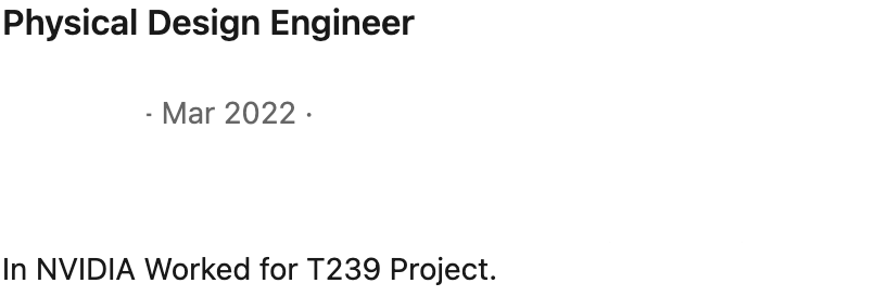
Design contracts ending: At least some designers left the T239 project in March 2022, about a month after the NVN2 hack
Electrical verification: Immediately after that, electrical verification began - this is a process to validate complete chips, implying that the design was complete and sampling had begun
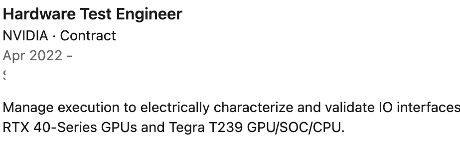
This strongly matches with the timing of Linux commits implying that the SOC design was locked and chip sampling began in April.
Additional LinkedIn profiles have confirmed that T239 and it's File Decompression Engine were designed specifically for "video games", but these profiles are no longer public (and why we have obscured details here).
The NVN2 Hack
Again, we will not be linking to or discussing the hack in depth here. However, there are a few bits worth noting.
The data breach happened in late February 2022. Considering the strong evidence that the chip was sampling in April 2022, it seems highly likely that the hack represents a close-to-final description of T239.
Some members of the community have extracted data out of this hack. Almost universally this just confirms information discovered in Nvidia's Linux code or it's documentation - that it is a full fat Ampere chip with all the expected DLSS/RT features, that some power saving Ada features have been backported, but not DLSS 3, and that T239 uses LPDDR5 RAM with a 128-bit memory bus.
The only significant piece of data that that has been extracted from the hack that isn't in the Linux drops is that T239 features 1536 CUDA Cores. There is circumstantial evidence however, as 1536 is a "magic" number in both the Ampere and Ada architectures, as it is the number of CUDA cores in a "full" Graphics Processing Cluster.
Intriguing Reports
Outside of the purely technical realm, there have been a few interesting tidbits of information which I think as sufficiently credible as to be worth considering.
The Spanish Devkit: In July, a Spanish leaker claimed that a studio in Spain had recently received a devkit. That leaker is not considered super credible, however, shortly after a Brazilian journalist who is considered credible independently confirmed this info. I have also confirmed it, but I'm just some asshole on the internet, so please, press X to doubt.
MoneyDJ: MoneyDJ is a well known Taiwanese financial outlet, and they have stated they expect a launch early next year for the next Switch. The reporter has a history with Nintendo and Foxconn, having previously leaked the OLED a month before its announcement. (Hongzhun is a subsidiary of Foxconn, who manufacture all Nintendo consoles since the GameCube). It is likely "launch" refers to the beginning of manufacturing and not to consumer release, regardless.
Microsoft/Activision: During the recent legal battles over Microsoft's acquisition of Activision, a number of references to new hardware have come up. The UK's regulatory authority released a summary document with references to new Nintendo hardware redacted (resulting in community nickname of REDACTED for the new device). Activision seems to have received an executive summary of the device from Nintendo under the heading of Switch NG. Reports about Activision confirming a PS4 level of power from this device are a misrepresentation of the actual in court conversation, but are roughly reflected by the specs discovered above.
What The Heck This Means
Nintendo's next device uses a mobile architecture (LPDDR5, for example), but able to connected to an external screen (DisplayPort), and is referred to as a "Switch NG" by partner studios. In other words, it is a new Switch.
The SOC design seems to have been finalized Spring 2022. Both supply chain leaks and dev leaks point toward a 2024 release. No significant information on new features - like new control schemes, cameras, etc - seems to exist.
How powerful is it? For layfolk
A rough last-gen performance level seems likely across the board. Considering the performance gap between the Xbox One and the PS4, that's a broader range than might seem obvious, but last gen ports shouldn't be exceptionally challenging.
DLSS 2.0 is a much more efficient 4K upscaler than the checkerboard technique used by the last gen pro consoles. Even if the Switch NG is well below the PS4 Pro level of power, well considered ports should be able to take advantage of this to have comparable - if not identical - 4K experiences.
How powerful is it? Some educated guesses
We can make a number of spec guesses based on the data we already have.
A 128-bit LPDDR5 bus would provide 102 GB/s of memory bandwidth, at max MC clocks, and 68 GB/s at slower clocks.
Notebookcheck provides a handy tool for querying a large data set of shipped phones and laptops. We can see that 4GB 64-bit LPDDR5 memory modules don't seem to have shipped. Unless Nintendo chooses to purchase a custom RAM solution, 12GB would actually be cheaper than 8GB.
We can also see that eMMC storage is dying out, and modern phone SOCs don't seem to include the eMMC controller. UFS based internal storage seems extremely likely, especially considering the number of available PCIe lanes.
Nvidia provides a handy tool for generating Orin power consumption data, allowing us to guess at peak power efficiency for the GPU. Below 400 MHz, very little power is saved, and Nintendo would be better served (battery life wise) to remove CUDA cores, rather than lower clock speeds. This seems like a reasonable floor. Past 540 MHz, the GPU becomes rapidly less efficient, so that seems like a reasonable ceiling for handheld.
FP32 TFLOPS for Ampere and Ada GPUs is CUDA Count * Clock Speed * 2. We can assume roughly a doubled GPU clock in handheld mode.
CPU curves are more difficult to extract, but a similar floor occurs around 1 GHz, and ceiling around 1.4 GHz.
The DLSS Programming Guide provides some useful benchmarks for DLSS across a range of cards and scaling modes, showing roughly how much "extra" performance you might need to take a game to 4K.
What about the Steam Deck? - a (lengthy) aside about power effeciency
The Steam Deck is widely described as "a handheld PS4", and it is also widely considered to be much larger and more power hungry than Nintendo would ever go, so how is "PS4 comparable" possible?
The key is the CPU cores, and this cannot be emphasized enough. Valve is forced to go with a power inefficient design for PC compatibility reasons.
Valve needs x86 CPUs in order to run PC games, and went with the Zen 2 cores that were available at the time from AMD. Zen 2 is an excellent, high performance CPU, but it is absolutely slaughtered in power efficiency by any modern ARM core. In head to head comparisons, the ARM N1 (a server class variant of the same A78 core in T239).
a Zen 2 core at 3 GHz typically draws 48% to 98% more power than a N1 core
Beyond that, the Steam Deck is actually kind of a beast compared to last gen consoles on the CPU side. Not only is the Zen 2 much more powerful per clock than the anemic Jaguar CPUs in those consoles, it's clocked much much higher, reaching as high 3.5Ghz across it's 8 threads.
T239's A78C cores simply don't need to reach those outrageous clock speeds to achieve "last gen" performance. Between the lower clock speeds and the more efficient cores, there is an excellent battery life advantage here. But there are bang on effects of that decision.
The Zen2 cores are much larger than the ARM cores. A single 8 core cluster of Zen2 CPUs is 125 mm² on TSMC 7, but on the same process node, the entire Snapdragon 855 SOC - including an 8 core CPU cluster, the GPU, an all the associated memory and storage controllers - is only 74 mm² .
This matters because it leaves less room on Valve's APU for the GPU itself. Valve has gone for 8 RDNA 2 Compute Units, where Nintendo has gone for 12 of Ampere's equivalent Streaming Multiprocessors. In general, this wider design at lower clock speeds is much more power efficient.
Valve's 8 CUs reaches 1.0 TFLOPS at a 1GHz clock speed. T239's 12 SMs achieves the same level of performance at 350Mhz.