Cpu Spread

⚡ ALL INFORMATION CLICK HERE 👈🏻👈🏻👈🏻
Cpu Spread
Dec 15, 2011
Written by: MarshallR
Articles:
ACI Guides Guides Overclocking Hands On Motherboards Overclocking
Article Tags:
Guides Hands On
Diving deep into the revolutionary dual-screen Zephyrus Duo 15
Hands-on: Elite gaming and creative power collide in the slim ROG Zephyrus S15
Guide: Scenario Profiles get your ROG system ready to work or play with the right settings every time
Originally written by Raja from ASUS North America, this guide should help new Rampage IV Extreme owners get to grips with their UEFI options a little easier, while still going into intimate depth of each setting. Let us know if you have questions or comments in the forums or on our ROG Facebook page , or over at ASUS North America's , or in the ROG forums .
The ROG team have put an extensive amount of work into UEFI for the R4E. Most of the settings will not need manual adjustment at all unless you are chasing every last MHz from your system. This guide will focus on the meaning of most of the important settings and offer some insight as to when adjustments can help. We will follow up with a quick setup guide for beginners also.
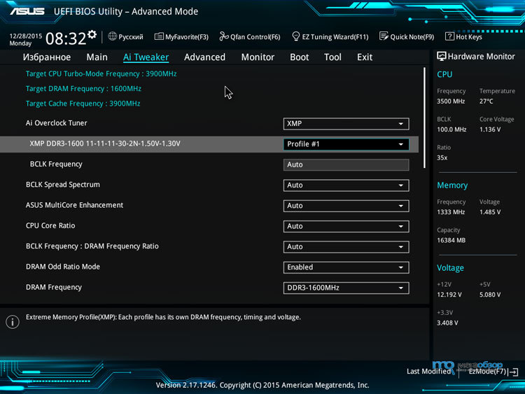
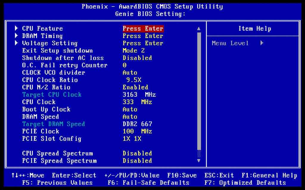
Upon entering UEFI BIOS, we navigate to the AI Tweaker menu:
Load Normal/Gamers/Extreme OC Profile: Each of these settings contains a pre-set that sets system bus frequencies and voltages for a quick starting point if you’re new to overclocking. The Normal profile will overclock your CPU to 4.375 GHz, the Gamer profile to 4.7 GHz. The Extreme profiles are for users that are utilizing Sub-zero cooling or chilled watercooling as both will set processor frequency at around 4.9GHz. With all of these profiles, active cooling of the onboard heatsinks is required.
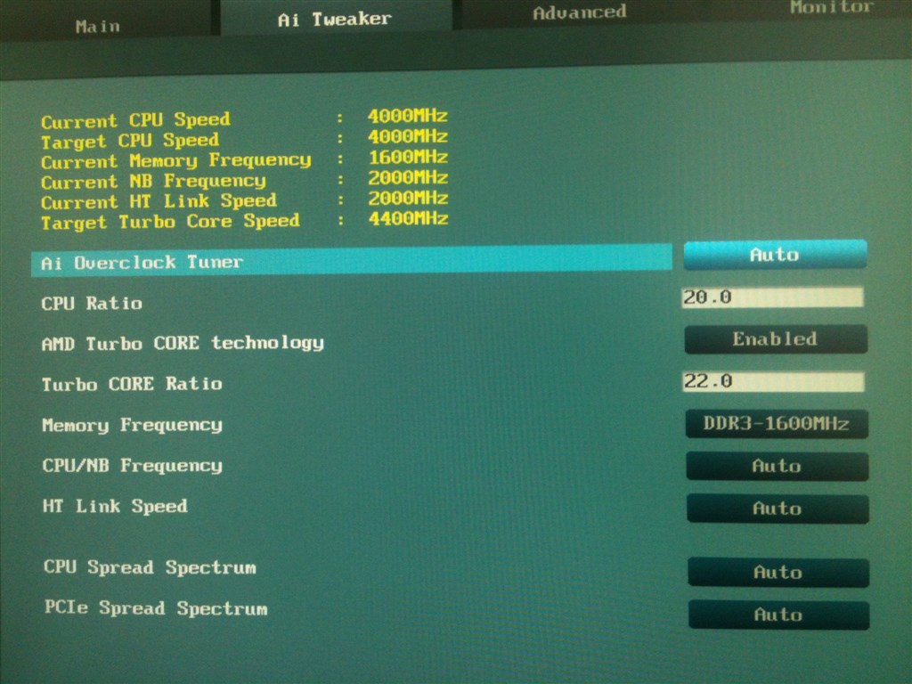
Ai Overclock Tuner: Options are Auto, Manual and X.M.P.
Auto: This is the default setting, and needs to be changed to Manual if you wish to change BCLK (BCLK is the base reference frequency from which processor and other system bus frequencies are derived).
X.M.P: Extreme memory profile, use this option if you have Sandy Bridge qualified XMP memory. X.M.P. profiles contain pre-sets for system buses and in some cases voltages. If the specified speed of the DIMMs is greater than the supported memory frequency of the platform, a platform specific X.M.P. profile option becomes mandatory because processor core and memory controller voltage requirements vary from architecture to architecture. High-speed enthusiast memory kits manufactured before the inception of the Sandybridge platform may not contain the necessary/adequate voltage offset settings for the system to be completely stable. In such instances, manual adjustments of memory controller voltage and memory timings may be necessary.
Selecting the X.M.P setting opens up options for X.M.P profile selection (the kit may contain more than one X.M.P profile), and also opens up the BCLK option for changing system bus frequency. Note that memory operating frequency and maximum CPU operating frequency are shown towards the top of the Ai Tweaker menu, while memory timings and voltage are displayed next to the XMP profile selection box.
CPU Level Up: Allows us to select a pre-set profile that contains voltage and bus adjustments to apply a mild overclock to the system. Use this setting if you do not wish to overclock the system manually.
BCLK Frequency: This function becomes available if X.M.P or Ai Overclock Tuner “Manual” are selected. The base BCLK frequency is 100MHz. The CPU core frequency is derived via multiplication with the Turbo Ratio setting (final frequency is displayed at the top-left of the Ai Tweaker menu).
Bear in mind that the adjustment margin for this setting is not large - most processors have a range of 7 MHz +/- the base frequency. For example, if using a CPU Strap setting of 100MHz, then the approximate maximum BCLK for some CPUs is 107.0 MHz. If using the 125 MHz strap, then we’d expect a maximum in the 130 BCLK range.
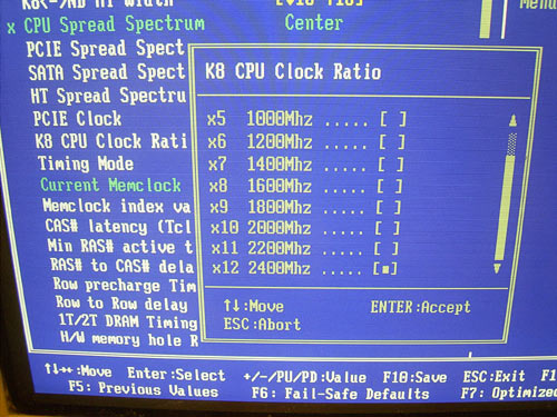
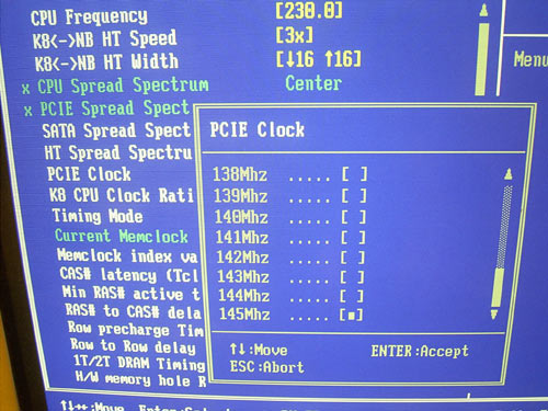
CPU Strap: This setting multiplies BCLK to increase CPU frequency asynchronously from all other bus frequencies giving us more granularity to maximise processor and memory overclocking. Available settings are 100, 125, 166 and 250 MHz. For most CPUs the usable “straps” are 100 and 125 only. If using 166, try starting at 155 and see if the board will POST. If not, then you are likely limited to using 100 and 125 only.
Clockgen Full Reset: Re-initializes the on-board clock generator when bus frequencies or multipliers are changed. A setting of Enabled is recommended for all normal syste use. Disable only to experiment with memory stability when making changes to BCLK.
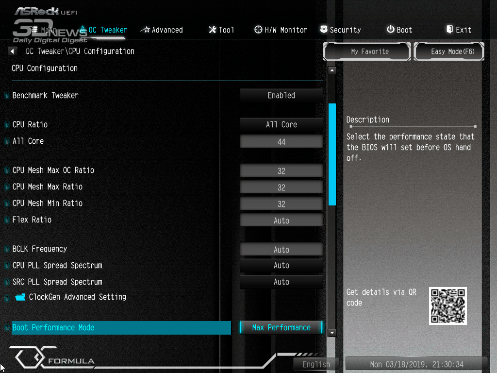
Turbo Ratio: Options are “Auto”, “By All Cores” and “By Per Core”. A description of these settings is provided in the right-hand column of the UEFI BIOS and can be seen when the Turbo Ratio setting is selected. Note that if overclocking past 4.5GHz, it can be beneficial to turn disable the Anti Surge Support setting in the Monitor section of UEFI to prevent power shut-off due to Super IO polling.
By All Cores: This sets the CPU core frequency multiplier; multiplied by BCLK to give the target CPU frequency (under full load conditions if SpeedStep is active). “Auto”: Stock CPU multiplier Ratio used. Manual numerical entry of the desired Turbo Ratio is accepted.
Per Core: Allows setting the maximum Turbo multiplier of each physical processor core.
The available multiplier range is limited by both processor model and the ability of each CPU.
CPU Clock Gen Filter: A setting of Auto is recommened for most overclocking. For memory speeds over DDR3-2200 use 10UF, for speeds over DDR3-2400 use 20UF. If using the 166 strap then a setting of Disabled is recommended.
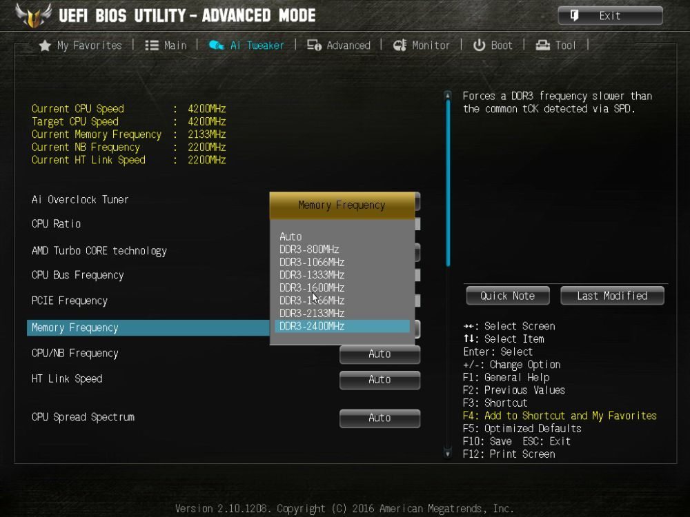
Memory Frequency: “Auto” will automatically select a memory multiplier ratio according to memory module SPD (Serial Presence Detect). Manual selection of the available memory frequency multiplier ratios is possible and works according to the abilities of the DRAM and processor. Granular control of memory frequency is available by manipulating BCLK, while the base frequency of each divider is offset by changing the CPU strap settings (within functional limits).
EPU Power Saving Mode: When “Enabled” is selected, utilizes power phase management based upon system loading to reduce system power consumption. A setting of “Disabled” is recommended for heavy overclocking.
DRAM Timing Control: Takes us to the DRAM timing sub-menu, where all primary, secondary and tertiary memory timings can be set:
Load Elpida Hyper/ Tight PSC/Loose PSC RAW MHz Profile:? These profiles contain presets for the entire DRAM timing section and allow quick setup to facilitate overclocking or benchmarking. If you are using PSC or Elpida Hyper based modules, then try these profiles as a starting point. If overclocking with 64GB of memory, then using the RAW MHz Profile may be beneficial if you are experiencing any instability.
Rampage Tweak: A setting of Mode 2 is recommended for overclocking memory over DDR3-2000 or if using 64GB of memory.
Memory timings will automatically be offset according to memory module SPD and memory frequency. Should you wish to make manual adjustments, the primary settings are the most important for overall memory performance. Most timings are set in DRAM clock cycles, hence a lower value results in a more aggressive setting (unless otherwise stated).
As always, performance increases from memory tuning are marginal and are generally only noticeable during synthetic benchmarks. Either way, voltage adjustments to VDIMM, VCCSA and to a lesser extent CPU Core Voltage may be necessary to facilitate tighter timings.
CAS: Column Address Strobe, defines the time it takes for data to be ready for burst after a read command is issued. As CAS factors in almost every read transaction, it is considered to be the most important timing in relation to memory read performance.
To calculate the actual time period denoted by the number of clock cycles set for CAS we can use the following formula:
tCAS in Nano seconds=(CAS*2000)/Memory Frequency
This same formula can be applied to all memory timings that are set in DRAM clock cycles.
DRAM RAS TO CAS Latency: Also known as tRCD. Defines the time it takes to complete a row access after an activate command is issued to a rank of memory. This timing is of secondary importance behind CAS as memory is divided into rows and columns (each row contains 1024 column addresses). Once a row has been accessed, multiple CAS requests can be sent to the row the read or write data. While a row is “open” it is referred to as an open page. Up to eight pages can be open at any one time on a rank (a rank is one side of a memory module) of memory.
DRAM RAS# PRE Time: Also known as tRP.Defines the number of DRAM clock cycles it takes to precharge a row after a page close command is issued in preparation for the next row access to the same physical bank. As multiple pages can be open on a rank before a page close command is issued the impact of tRP towards memory performance is not as prevalent as CAS or tRCD - although the impact does increase if multiple page open and close requests are sent to the same memory IC and to a lesser extent rank (there are 8 physical ICs per rank and only one page can be open per IC at a time, making up the total of 8 open pages per rank simultaneously).
DRAM RAS Active Time: Also known as tRAS. This setting defines the number of DRAM cycles that elapse before a precharge command can be issued. The minimum clock cycles tRAS should be set to is the sum of CAS+tRCD+tRTP.
DRAM Command Mode: Also known as Command Rate. Specifies the number of DRAM clock cycles that elapse between issuing commands to the DIMMs after a chip select. The impact of Command Rate on performance can vary. For example, if most of the data requested by the CPU is in the same row, the impact of Command Rate becomes negligible. If however the banks in a rank have no open pages, and multiple banks need to be opened on that rank or across ranks, the impact of Command Rate increases.
Most DRAM module densities will operate fine with a 1N Command Rate. Memory modules containing older DRAM IC types may however need a 2N Command Rate.
Latency Boundary: Use a setting of Nearer for most modules. For older DRAM ICs a setting of Further may be beneficial.
DRAM RAS to RAS Delay: Also known as tRRD (activate to activate delay). Specifiesthe number of DRAM clock cycles between consecutive Activate (ACT) commands to different banks of memory on the same physical rank. The minimum spacing allowed at the chipset level is 4 DRAM clocks.
DRAM Ref Cycle Time: Also known as tRFC. Specifies the number of DRAM clocks that must elapse before a command can be issued to the DIMMs after a DRAM cell refresh.
DRAM Write Recovery Time: Defines the number of clock cycles that must elapse between a memory write operation and a precharge command. Most DRAM configurations will operate with a setting of 9 clocks up to DDR3-2500. Change to 12~16 clocks if experiencing instability.
DRAM Read to Precharge Time: Also known as tRTP. Specifies the spacing between the issuing of a read command and tRP (precharge) when a read is followed by a page close request. The minimum possible spacing is limited by DDR3 burst length which is 4 DRAM clocks. Most 2GB memory modules will operate fine with a setting of 4~6 clocks up to speeds of DDR3-2000 (depending upon the number of DIMMs used in tandem). High performance 4GB DIMMs (DDR3-2000+) can handle a setting of 4 clocks provided you are running 8GB of memory in total and that the processor memory controller is capable. If running more than 8GB expect to relax tRTP as memory frequency is increased.
DRAM Four Activate Window: Also known as tFAW. This timing specifies the number of DRAM clocks that must elapse before more than four Activate commands can be sent to the same rank. The minimum spacing is tRRD*4, and since we know that the minimum value of tRRD is 4 clocks, we know that the minimum value for tFAW at the chipset level is 16 DRAM clocks.
As the effects of tFAW spacing are only realised after four Activates to the same DIMM, the overall performance impact of tFAW is not large, however, benchmarks like Super Pi 32m can benefit by setting tFAW to the minimum possible value.
As with tRRD, setting tFAW below its lowest possible value will result in the memory controller reverting to the lowest possible value (16 DRAM clocks or tRRD * 4).
DRAM Write to Read Delay: Also known as tWTR. Sets the number of DRAM clocks to wait before issuing a read command after a write command. The minimum spacing is 4 clocks. As with tRTP this value may need to be increased according to memory density and memory frequency.
DRAM Write Latency: For the most part this setting can be left to Auto, and generally will default to Read CAS -1. So if CAS is set to 8 for example, Write CAS may default to 7. To facilitate stability at higher DDR3 speeds (over DDR3-2133) and if using 64GB of memory, then increasing Write CAS by 1~2 clocks should help at the expense of memory write speed performance. Older DIMMs may not POST if Write CAS is set over 8 clocks, so you will need to limit write IO by relaxing some of the Write to Write timings such as tWWDD and tWWDR and/or increasing VDIMM.
Most of these timings can be left on AUTO unless tweaking for SuperPi 32M.
tRRDR: Sets the read to read delay where the subsequent read requires the access of a different rank on the same DIMM. 3 clocks will work with most configurations at high memory frequencies. Only needs adjustment when double-sided DIMMs are used.
tRRDD: Sets the read to read delay where the subsequent read requires the access of a different DIMM. 3 clocks will work with most configurations.
tWWDR: Sets the write to write delay where the subsequent write command requires the access of a different rank on the same DIMM.
tWWDD: Sets the write to write delay where the subsequent write requires the access of a different DIMM. 3 clocks will work with most configurations.
tRWDR: Sets the delay period between a read command that is followed by a write command; where the write command requires the access of data from a different rank. A setting of 3 clocks suits most DIMM configurations all the way to DDR3-2133. Relax to 5~7 clocks only if you are experiencing stability issues when running in excess of 8GB of memory over DDR3-2300.
tRWDD: Sets the delay period between a read command that is followed by a write command; where the write command requires the access of data from a different rank or DIMM. A setting of 3 clocks suits most DIMM configurations all the way to DDR3-2133. Relax to 5~7 clocks only if you are experiencing stability issues when running in excess of 8GB of memory over DDR3-2300.
tWRDR: Sets the delay period between a write command that is followed by a read command; where the read command requires the access of data from a different rank. A value of 1 is possible on high performance memory. For higher density modules this value may need relaxing to 5~7 clocks as memory frequency is increased.
tWRDD: Sets the delay period between a write command that is followed by a read command; where the read command requires the access of data from a different DIMM. A value of 1 is possible on high performance memory. For higher density modules this value may need relaxing to 5~6 clocks as memory frequency is increased.
tRWSR: Sets the read to write delay timing where the write follows a read on the same rank. Can be left to 3 clocks for most configurations. 1~2 clocks may be possible at lower memory frequencies depending upon module density (sub DDR3-1866). If experiencing instability after adjusting all other timings, then try a setting of 5~7 clocks.
tCCD: Sets the read to read delay where the subsequent read accesses a different column after a four clock burst. The minimum internal spacing is 4 DRAM clocks, if a setting of 0 is used the chipset will default to 4 clocks. For all overclocking, it is recommended that this setting is left at 4 clocks to maintain read performance.
DRAM RTL (all ranks and channels): Also known Round Trip Latency. RTL denotes the number of clock cycles it takes for a data to arrive at the memory controller after a read CAS command is issued. This value is specified in memory controller clock cycles (not DRAM clock cycles). On the Sandybridge architecture these values can safely be left on AUTO most of the time and do not need manual adjustment.
Should you wish to experiment, note that DRAM IOL should be changed, too. If delaying RTL, then delay IOL by 1~2 clocks for example.
DRAM CLK Period: Can really affect performance and yet overclocking at the same time. A centered value of around 5 or 7 usually gives best performance but it may not be that great for overclocking. A value of 3 or 7 can be good for Command Rate 1T overclocking.
Enhanced Training (CHA-CHD): There is no definite best setting for Enhanced Training, usually though disabling it helps with overclocking on R4E
MCH Duty Sense (CHA-CHD): Again no definite best setting for MCH Duty Sense though using a lower value on CHA and CHC than the one used on CHB and CHD may be helpful. 15-19 perhaps are good values to experiment with.
Receiver Slew: Leave on Auto for most overclocking. Try a setting of Normal if experiencing instability when running memory over DDR3-2133.
Transmitter Slew: Leave on Auto for most overclocking. Try a setting of Normal if experiencing instability when running memory over DDR3-2133.
MCH Recheck: Forces memory to be rechecked to ensure all DIMMs are mapped. Leave on Auto unless experiencing instability.
RC Warm Boot Fast: Disables memory training when Enabled. If running at speeds over DDR3-2133, then Enable this setting once the memory is stable. Drift in memory training parameters may result in instability if this setting is left enabled if the system is booted multiple times or during sub-zero cooled benchmarking sessions. For all other purposes leave on Auto or Disabled.
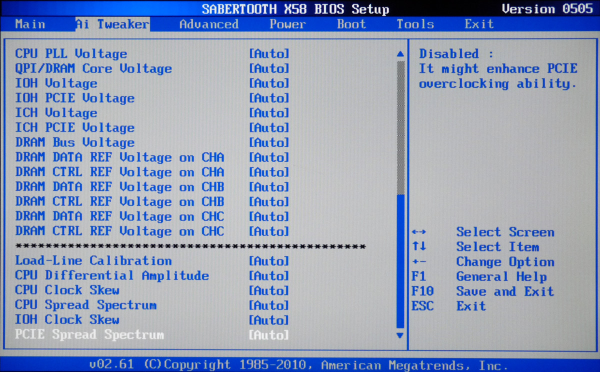
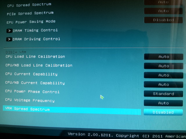
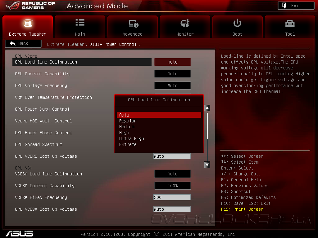
VCore Load-Line Calibration: Sets a margin between idle and full processor load voltage to compensate for overshoot. To clarify; overshoot is a short duration voltage excursion beyond applied processor VID. We recommend a setting of Medium for most overclocking.
CPU Current Capability: Increases the power threshold before over-current protection limits power (either by shut-off or throttling). A setting of 180% is ample for all types of overclocking.
CPU Voltage Frequency: Sets the switching frequency of the power FETs supplying processor Vcore. Lower switching frequencies lead to a higher VRM efficiency (small power saving) and lower VRM operating temperatures. Setting a higher switching frequency aids transient response (the recovery of voltage to the applied level after a load condition) – at the expense of heat.
VRM Over-temperature Protection: Monitors CPU VRM MOSFET temperatures and if the temperature breaches a certain threshold either throttles the processor clock frequency to reduce current consumption or shuts-down the motherboard to prevent VRM failure. May be turned off is using sub-zero cooling on the processor. For all other purposes, leave this setting enabled and provide active cooling over the CPU VRM heatsink to keep temperatures in-check.
CPU Power Duty Control: Sets the conditions for load balancing across phases. “T.Probe” monitors phase thermal conditions and balances load accordingly. “Extreme” balances the current load across all FETs irrespective of thermal conditions.
VCore MOS volt. Control: Sets the CPU VRM driver output voltage. This setting can be left on Auto for all overclocking. If wishing to experiment with manual settings then bear in mind that most FETs used on motherboards are generally optimised for a VGS of 5V, so a setting of 7V is generally optimal and should provide the best voltage swing.
CPU Power Phase Control: Sets the load dependant phase switching conditions; the VRM is made up of multiple phases (each phase has at least two FETs). During light-load conditions FETs can be switched off to save power. “Standard” and “Optimized” are adequate for most loading conditions and required if you wish to use Offset Mode for Vcore. If pushing processors past 4.8GHz, then Extreme or “Manual” with “Ultra-Fast” is recommended.
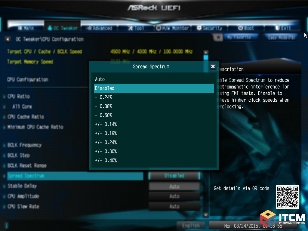
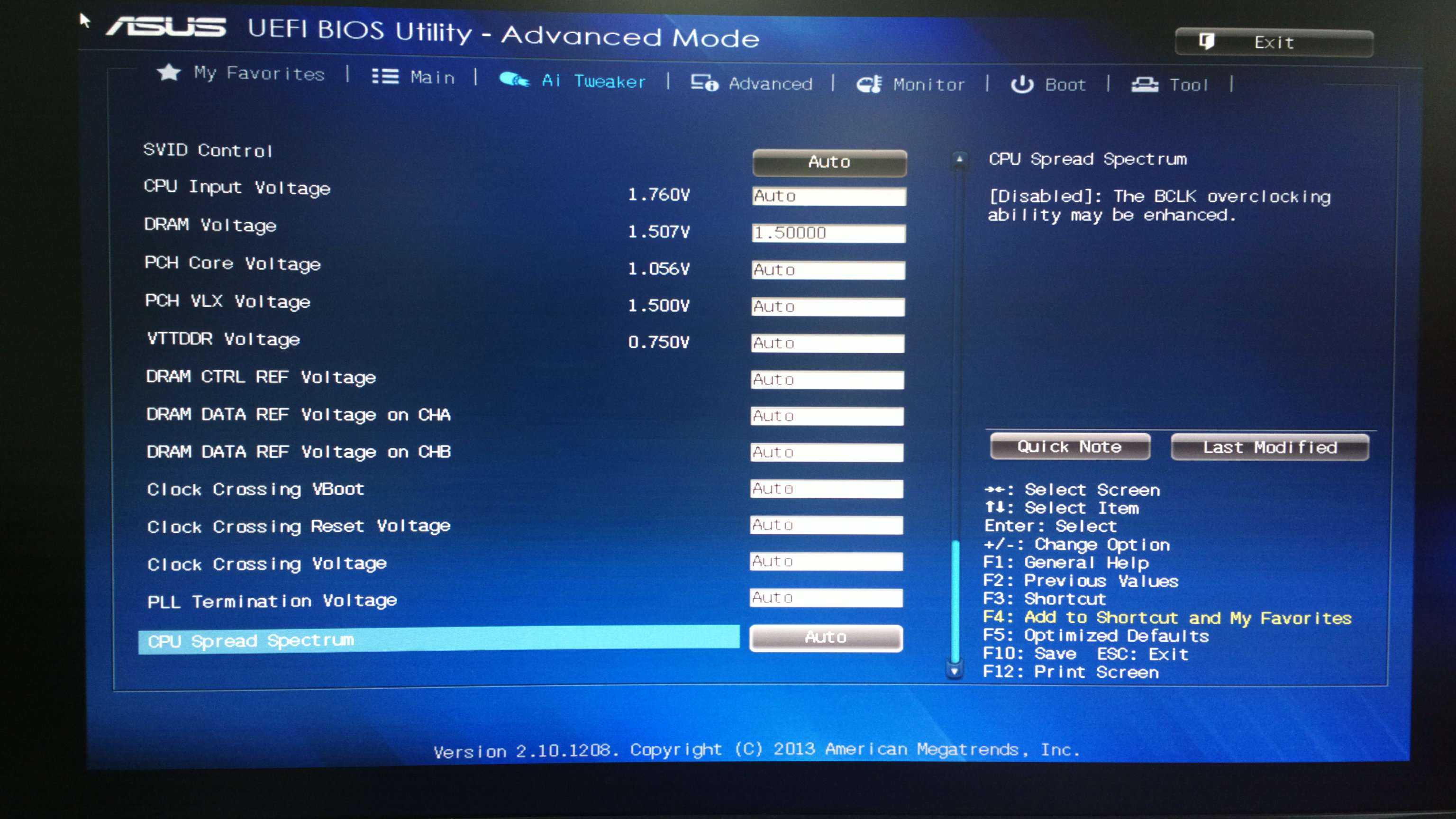
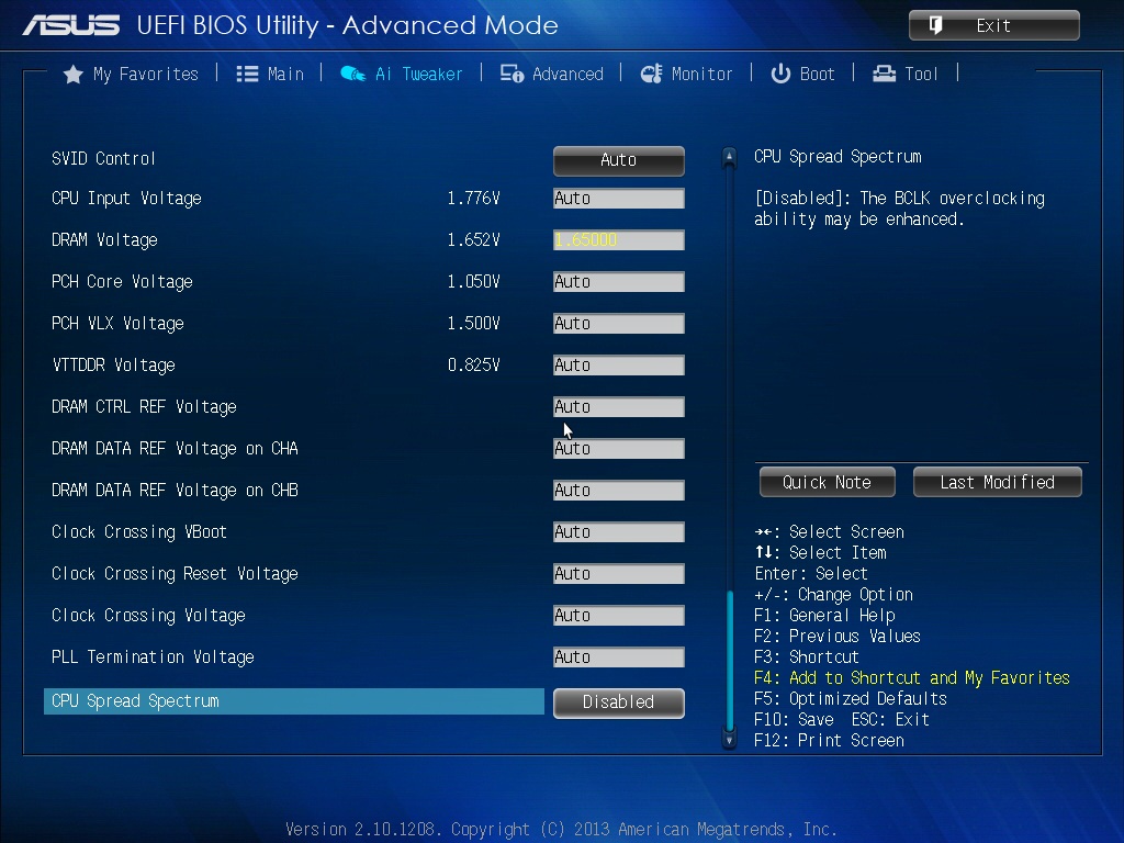
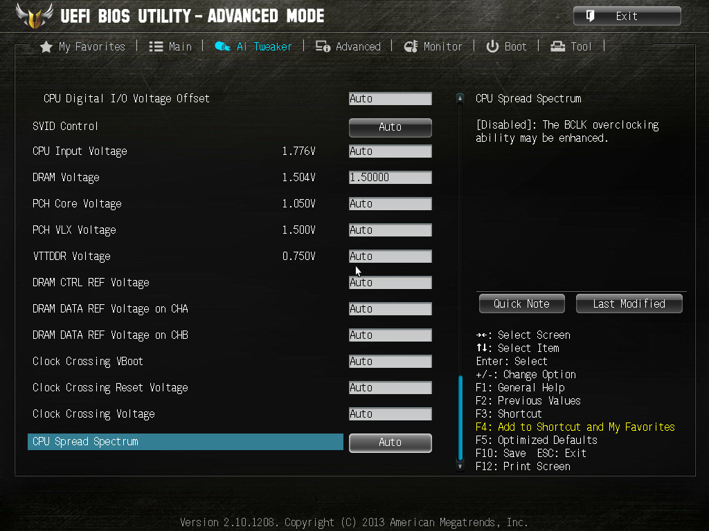
CPU Spread Spectrum: Modulates the CPU VRM clock signal to reduce the peak magnitude of radiated noise emission levels (may be of use during audio recording/playback from the analogue audio outputs) . This setting should be used at stock system operating parameters only.
CPU Vcore Boot Up Voltage: Can be left at Auto for normal use. If benchmarking, then setting a lower or higher boot-up voltage for the CPU can aid in ensuring the system POSTs – experiment if experiencing non-POST situations only.
VCCSA Load-Line Calibration: Sets a margin between idle and full System Agent load voltage to compensate for overshoot. We recommend a setting of Medium for most overclocking.
VCCSA Current Capability: Increases the power threshold before over-current protection limits power. Increase to 140% if running 64GB of memory or if running memory speeds in excess of DDR3-2133.
VCCSA Fixed Frequency: Sets the switching frequency of the power FETs supplying the processor System Agent. Lower switching frequencies lead to a higher VRM efficiency (small power saving) and lower VRM operating temperatures. Setting a higher switching frequency aids transient response (the recovery of voltage to the applied level after a load condition) – at the expense of heat.
CPU VCCSA Boot Up Voltage: Can be left at Auto for normal use. If benchmarking, then setting a lower or higher boot-up voltage for the CPU can aid in ensuring the system POSTs at higher DRAM operat8ing frequencies – experiment if experiencing non-POST situations only.
CPU VTT Switching Freq: Sets the switching frequency of the power FETs supplying VTT. Lower switching frequencies lead to a higher VRM efficiency (small power saving) and lower VRM operating temperatures. Setting a higher switching frequency aids transient response (the recovery of voltage to the applied level after a load condition) – at the expense of heat.
CPU VTT Over-Current Protection: Increases the power threshold before over-current protection limits power. Increase when overclocking the processor past 4.5GHz.
DRAM-AB/CD Current Capability: Increases the power threshold before over-current protection limits power. Increase to 130% if using 64GB of memory past DDR3-1866, or when running 8GB modules over DDR3-2133.
DRAM-AB/CD Voltage Frequency: Sets the switching frequency of the power FETs supplying DRAM Voltage. Lower switching frequencies lead to a higher VRM efficiency (small power saving) and lower VRM operating temperatures. Setting a higher switching frequency aids transient response (the recovery of voltage to the applied level after a load condition) – at the expense of heat. Experimentation at various switching frequencies (higher and lower) at higher DDR3 speeds may be beneficial towards aiding stability.
DRAM-AB/CD Power Phase Control: Can safely be left at Auto for most loading conditions. For overclocking 64GB of memory, a setting of Extreme is recommended.
PCH 1.1v Switching Freq: Can be left on Auto for most overclocking. If running higher BCLKs, you may wish to alter switching frequency and see if it impacts stability.
CPU Performance Settings: This sub-menu contains SpeedStep, non Turbo multiplier ratios and CPU power settings. All settings can be left at Auto for most overclocking.
GPU.DIMM Post: opens a sub-page which shows how many GPUs are inserted into the PCIe slots and how many DIMMs are being used. If there are any peripheral issues or system bus speeds have been increased too far, one of the GPUs or memory modules may not show in the GPU DIMM Post screen – a quick glance here can save a lot of head-scratching.
A new feature for the RIVE is PCIe Lane Simulator. A sub-menu allows you to select occupied slots and then shows lane allocation accordingly in case you want to ensure optimal lane bandwidth to your peripherals.
Extreme OV: Leave at disabled unless you need to use over 1.60Vcore for benchmarking.
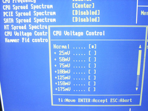
CPU Voltage: Two options here. The first is “Manual Mode”, which allows us to set a ‘static’ level of voltage for the CPU. The second mode is “Offset Mode”, for which we have covered the usage of here.
BCLK Skew: The sweet spot for BCLK Skew on this CPU is -2 bundled with -20 on PCIE CLK Skew. A good match in these 2 skews can help with BCLK/DRAM/Overall OC stability and help reduce Vcore requirements at a given operating frequency.
VTT CPU Voltage & 2 VTTCPU Voltage: To let users over-volt part of the CPU VTT that affects OC without over-volting the part of VTT that does not affect OC, we split up VTT rails to VTT and Secondary VTT.
VTT over-volting helps with DRAM and BCLK Overclocking. Secondary VTT does not. However, try to maintain at most a 300mv delta between both voltages for stability. 1.40v is fine on these CPUs. 1.35v is sufficient most of the time.
CPU VCCSA Voltage: Two options here. The first is “Manual Mode”, which allows us to set a ‘static’ level of voltage for the System Agent. The second mode is “Offset Mode”, which works on the same principals as Vcore Offset Mode. VCCSA has a direct impact on memory stability, so will need icnreasing if you are running high density modules and/or overclocking the memory controller.
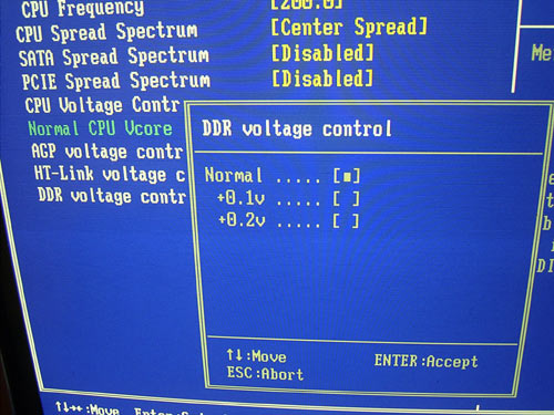
DRAM Voltage (CHA, CHB & CHC, CHD): Sets DRAM voltage for the memory. Set according to memory vendor specifications or alter to facilitate over/underclocking.
CPU PLL Voltage: For most overclocking, the minimum voltage requirements will be centered around 1.80V. If using higher processor multiplier ratios or DRAM frequencies over DDR3 2200, then a small over-voltage here can aid stability.
PCH 1.1V Voltage: Can be left at stock for most overclocking. If running very high VCCSA and VTT, then over-volting this rail to maintain the same voltage delta may be beneficial.
VTTDDR Voltage: Leave at Auto unless experiencing instability with memory. As a starting point, set to 50% of DRAM voltage. So if DRAM voltage is 1.65V, then set ~ 0.825V here.
CPU & PCIe Spread Spectrum: Disable if overclocking as clock modulation can cause instability.
For Tweakers Paradise menus, we have added text into UEFI describing when to adjust parameters.
Big thanks to GSkill for providing us with the 16GB DDR3-2133 Ripjaws Z memory kit, F3-17000CL9Q-16GBZHD to help compile this guide!
©ASUSTeK Computer Inc. All rights reserved.
Spread spectrum on or off? - CPUs , Motherboards, and... - Linus Tech Tips
Rampage IV Extreme UEFI BIOS Guide For Overclocking | ROG - Republic of...
Complete BIOS Tuning Guide - " Spread Spectrum Control" - ASUS Striker II...
Question - Does spread spectrum clocking degrade a CPU 's performance and...
PCIE Spread Spectrum from The Tech ARP BIOS Guide! | Tech ARP
ASUS Striker II Extreme: Mucho Bang, Mucho Bucks
by Kris Boughton on April 11, 2008 7:00 AM EST
Posted in
Motherboards
Index
It's getting expensive…
ASUS Striker II Extreme Board Layout and Features
ASUS Striker II Extreme Specifications
Test System Configuration and Methodology
Overall System Performance with PCMark Vantage
Synthetic 3D Graphics Results
Game Testing - Crysis
Game Testing - Unreal Tournament 3
Game Testing - Company of Heroes: Opposing Fronts
Intel 45nm Quad-Core Overclocking
Memory Access Latency and Read Performance
Memory Write and Copy Performance
Complete BIOS Tuning Guide - "Extreme Tweaker"
Complete BIOS Tuning Guide - "Extreme Tweaker" (Cont'd)
Complete BIOS Tuning Guide - "Memory Timing Setting"
Complete BIOS Tuning Guide - "Over Voltage"
Complete BIOS Tuning Guide - "Over Voltage" (Cont'd)
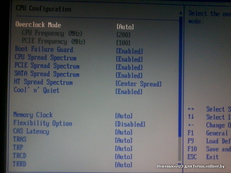
Complete BIOS Tuning Guide - "CPU Configuration"
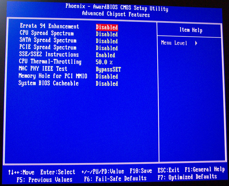
Complete BIOS Tuning Guide - "Spread Spectrum Control"
Final Thoughts and Recommendations
Complete BIOS Tuning Guide - "CPU Configuration"
Final Thoughts and Recommendations
Index
It's getting expensive…
ASUS Striker II Extreme Board Layout and Features
ASUS Striker II Extreme Specifications
Test System Configuration and Methodology
Overall System Performance with PCMark Vantage
Synthetic 3D Graphics Results
Game Testing - Crysis
Game Testing - Unreal Tournament 3
Game Testing - Company of Heroes: Opposing Fronts
Intel 45nm Quad-Core Overclocking
Memory Access Latency and Read Performance
Memory Write and Copy Performance
Complete BIOS Tuning Guide - "Extreme Tweaker"
Complete BIOS Tuning Guide - "Extreme Tweaker" (Cont'd)
Complete BIOS Tuning Guide - "Memory Timing Setting"
Complete BIOS Tuning Guide - "Over Voltage"
Complete BIOS Tuning Guide - "Over Voltage" (Cont'd)
Complete BIOS Tuning Guide - "CPU Configuration"
Complete BIOS Tuning Guide - "Spread Spectrum Control"
Final Thoughts and Recommendations
Complete BIOS Tuning Guide
- "Spread Spectrum Control"
Spread spectrum controls are really added
to motherboards for one purpose only - they are sometimes needed so that a device
for sale within the US can include a legitimate Declaration of Conformity stating
compliance with Part 15 of the Federal Communications Commission (FCC) Rules. This
stipulates that operation of the device (motherboard), (a) may not cause harmful
interference, and (b) must accept any interference received, including interference
that may cause undesired operation. Sales of electronic devices within the US require
the strict observation of all FCC rules and regulations.
As a general requirement, every motherboard
must be capable of generating and distributing more than one common clocking signal
used to coordinate latching times as needed for the transfer and receipt of data
across the many high-speed interfaces found in today's systems. Because it is uncommon
for different busses to share similar operating frequencies, and because each must
be kept independent of the others, a significant portion of motherboard resources
are spent locating, monitoring, and regulating these circuits. Each circuit must
include a reference frequency, or known base frequency, from which all other frequencies
can be derived. A local oscillator usual provides this functionality.
The problem is these oscillators can
sometimes cause electromagnetic interference (EMI) centered about their operating
frequencies. In an effort to prevent these types of undesired interferences the
FCC, an independent licensing organization for devices capable of transmitting electromagnetic
signals, either intended or otherwise, operating under the purview of the US government,
enacted "Rule 15," effectively limiting the output power of such devices.
Engineers, looking for a way to meet
regulation, began using a method for limiting such interferences called spread spectrum
clocking. Spread spectrum clocking causes the signal regulation circuit to slightly
vary the frequency about the target frequency, effectively "spreading"
the power over a somewhat larger frequency band. The method of operation can be
used to control system output power below the FCC standard limits, allowing for
a claim of full compliance.
As you can imagine, even the smallest
variation in a clocking signal can be enough to create data transfer errors. The
fundamentals of overclocking demand the cleanest, purest signal possible, which
is why spread spectrum should always be disabled unless you have
a good reason to enable it. Ergo, CPU Spread Spectrum , PCIE
Spread Spectrum , MCP PCIE Spread Spectrum , SATA
Spread Spectrum , and LDT Spread Spectrum should all
be set to Disabled.
Naughty America 1080p
Lil Nasty
Porn Nasty Nymphos
Realitykings 24video Site
Ass 1