Checking out the Intricacies of PCB Production Refine
The manufacturing of Printed Circuit Boards (PCBs) is an intricate procedure that involves many steps, each essential to the capability and integrity of the end product. This post intends to provide a thorough overview of the PCB manufacturing procedure.
Design and Pre-Production Preparation: The journey of PCB manufacturing begins with design. Using customized software application, engineers produce an in-depth blueprint of the board, that includes the design of components, connections, and other critical attributes. This phase frequently involves a detailed evaluation to guarantee the layout satisfies all needs and is enhanced for manufacturability.
Developing the Substrate: The base product, commonly making up epoxy material and glass fiber (FR4), is prepared. This substrate types the core of the PCB, offering structural honesty and insulation in between the conductive layers.
Pattern Transfer: The next action includes moving the circuit layout onto the board. For internal layers of multilayer PCBs, this is done by finish the substratum with a light-sensitive film, onto which the style is printed making use of a UV light source. The unexposed locations are after that engraved away, leaving the copper pattern.
Layering and Lamination: In multilayer PCBs, several layers of material, consisting of copper foil and prepreg (pre-impregnated with resin) layers, are piled together. The pile is subjected to warm and pressure, causing the prepreg to thaw and bond the layers into a solitary, strong structure.
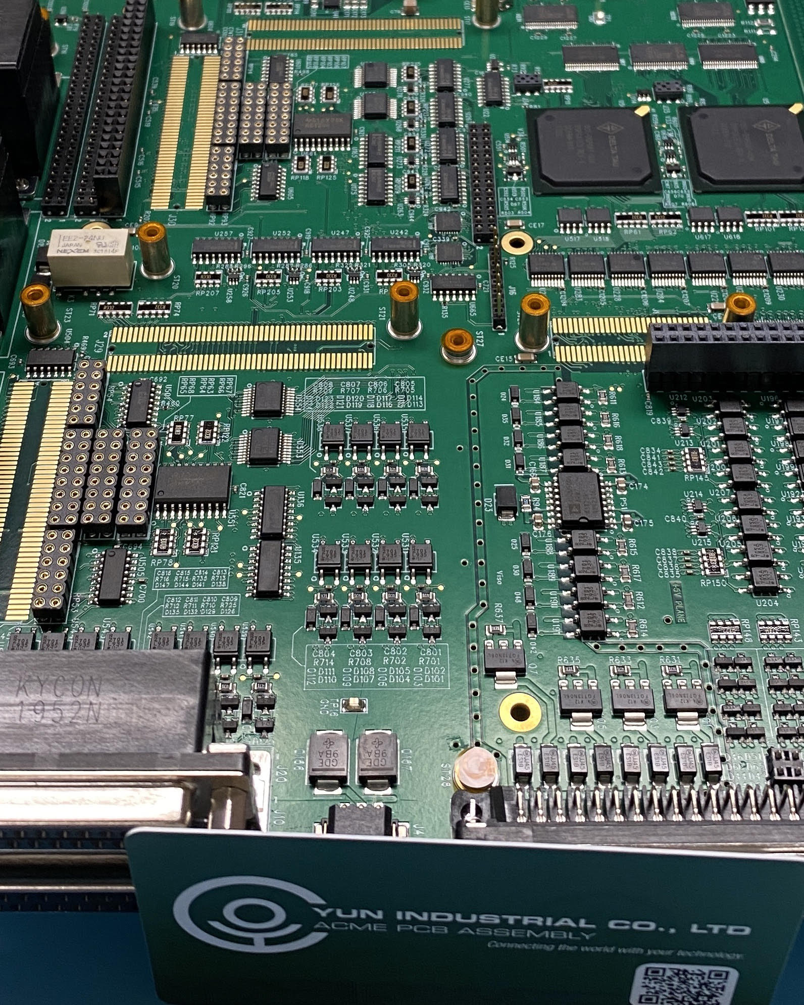
Boring: Openings are drilled into the PCB to permit the mounting of components and to produce vias, which are electrical connections between different layers of the board. This process requires high accuracy to make certain alignment and prevent damaging the internal layers.
Plating and Copper Deposition: The pierced PCBs go through electroplating, which deposits a thin layer of copper externally and inside the openings. This action is crucial for developing a good electrical connection via the vias.
Outer Layer Imaging and Growth: Comparable to the inner layers, the outer layers are coated with a photosensitive film. The outer layer style is then printed onto this movie, and the board is created to remove unexposed areas, exposing the copper pattern.
Etching: The subjected unwanted copper is etched away, leaving behind the desired circuit pattern. This action must be meticulously regulated to make certain the accuracy of the circuit layout.
Solder Mask Application: A solder mask is put on the board, covering the entire surface area with the exception of the locations where soldering will certainly happen, such as component pads and vias. This layer protects the copper from oxidation and protects against solder bridges between closely spaced conductive aspects.
Surface End Up: The PCB obtains a surface area coating, which can vary relying on the application. https://hitechcircuits.com include HASL (Hot Air Solder Progressing), ENIG (Electroless Nickel Immersion Gold), and OSP (Organic Solderability Preservatives). This finish protects the revealed copper circuitry and makes certain an excellent solderable surface.
Silkscreen Printing: Critical info such as part labels, examination factors, and logos are printed on the PCB utilizing a silkscreen procedure. This action adds a layer of ink to the board, normally on the component side, to assist in assembly and screening.
Evaluating and Quality Control: The final step in PCB manufacturing is screening and inspection. This can consist of Automated Optical Examination (AOI), X-ray evaluation, and electric testing to make sure the PCB meets all requirements and is without flaws.
Assembly and Final Inspection: If the PCB is to be delivered as a total assembly, parts are after that placed onto the board with procedures like SMT (Surface Mount Technology) or through-hole technology. A final assessment is performed to guarantee the assembly fulfills the called for standards.
Finally, PCB manufacturing is a detailed and specific process, needing a high degree of know-how and quality assurance. Each action, from layout to final evaluation, plays an important role in making certain the PCB performs as meant in its last application. As technology breakthroughs, the PCB manufacturing process continues to advance, suiting extra complex layouts and ingenious materials.