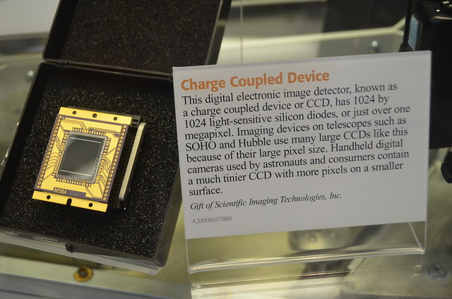
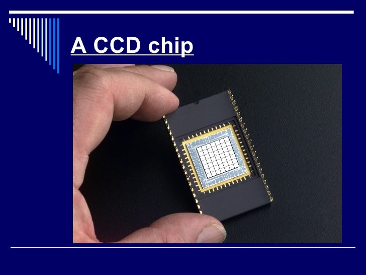
Charge Coupled Device

💣 👉🏻👉🏻👉🏻 ALL INFORMATION CLICK HERE 👈🏻👈🏻👈🏻
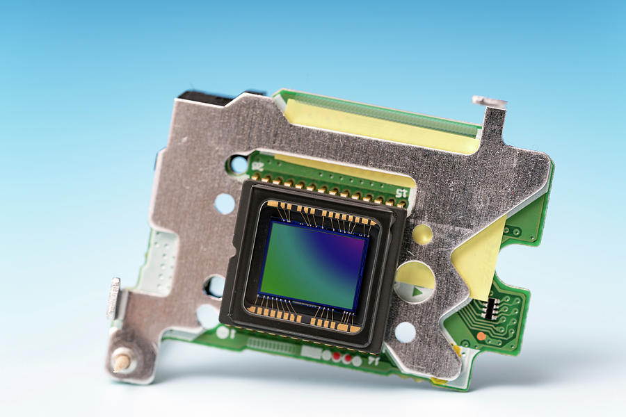
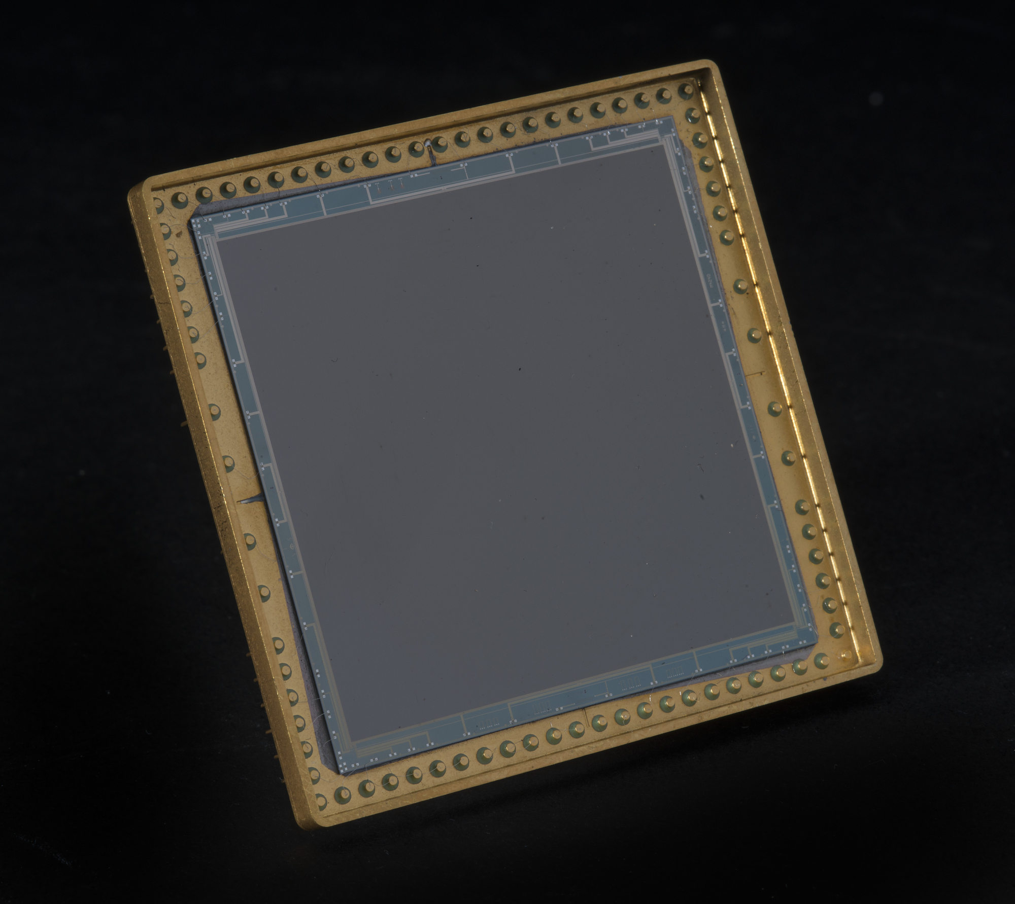
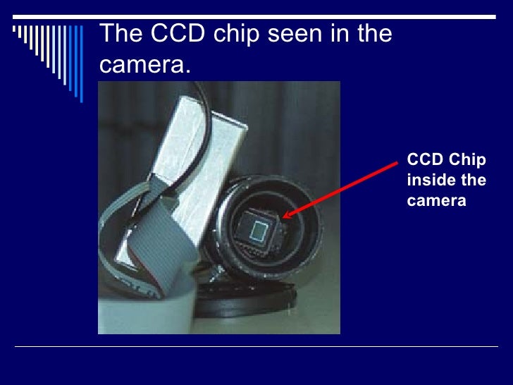
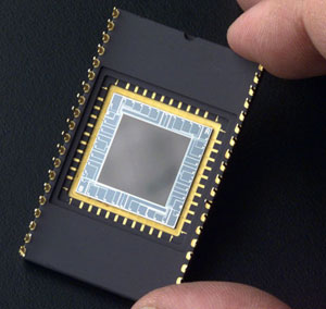
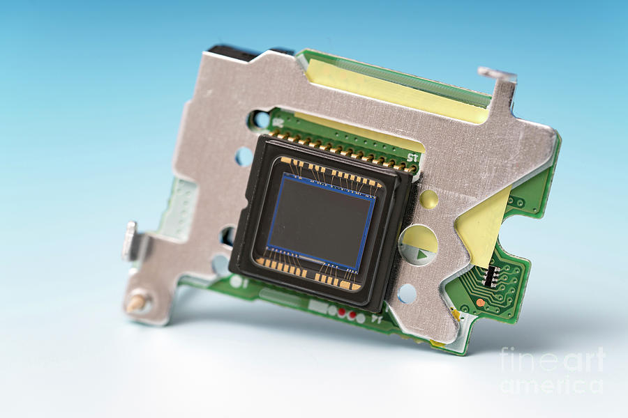
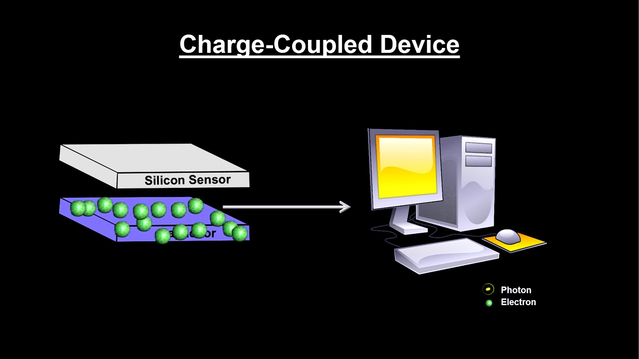
A charge-coupled device (CCD) is an integrated circuit containing an array of linked, or coupled, capacitors. Under the control of an external circuit, each capacitor can transfer its electric charge to a neighboring capacitor. CCD sensors are a major technology used in digital imaging.
In a CCD image sensor, pixels are represented by p-doped metal–oxide–semiconductor (MOS) capacitors. These MOS capacitors, the basic building blocks of a CCD,[1] are biased above the threshold for inversion when image acquisition begins, allowing the conversion of incoming photons into electron charges at the semiconductor-oxide interface; the CCD is then used to read out these charges. Although CCDs are not the only technology to allow for light detection, CCD image sensors are widely used in professional, medical, and scientific applications where high-quality image data are required. In applications with less exacting quality demands, such as consumer and professional digital cameras, active pixel sensors, also known as CMOS sensors (complementary MOS sensors), are generally used. However, the large quality advantage CCDs enjoyed early on has narrowed over time and since the late 2010s CMOS sensors are the dominant technology, having largely if not completely replaced CCD image sensors.
The basis for the CCD is the metal–oxide–semiconductor (MOS) structure,[2] with MOS capacitors being the basic building blocks of a CCD,[1][3] and a depleted MOS structure used as the photodetector in early CCD devices.[2][4]
In the late 1960s, Willard Boyle and George E. Smith at Bell Labs were researching MOS technology while working on semiconductor bubble memory. They realized that an electric charge was the analogy of the magnetic bubble and that it could be stored on a tiny MOS capacitor. As it was fairly straightforward to fabricate a series of MOS capacitors in a row, they connected a suitable voltage to them so that the charge could be stepped along from one to the next.[3] This led to the invention of the charge-coupled device by Boyle and Smith in 1969. They conceived of the design of what they termed, in their notebook, "Charge 'Bubble' Devices".[5][6]
The initial paper describing the concept in April 1970 listed possible uses as memory, a delay line, and an imaging device.[7] The device could also be used as a shift register. The essence of the design was the ability to transfer charge along the surface of a semiconductor from one storage capacitor to the next. The concept was similar in principle to the bucket-brigade device (BBD), which was developed at Philips Research Labs during the late 1960s.
The first experimental device demonstrating the principle was a row of closely spaced metal squares on an oxidized silicon surface electrically accessed by wire bonds. It was demonstrated by Gil Amelio, Michael Francis Tompsett and George Smith in April 1970.[8] This was the first experimental application of the CCD in image sensor technology, and used a depleted MOS structure as the photodetector.[2] The first patent (U.S. Patent 4,085,456) on the application of CCDs to imaging was assigned to Tompsett, who filed the application in 1971.[9]
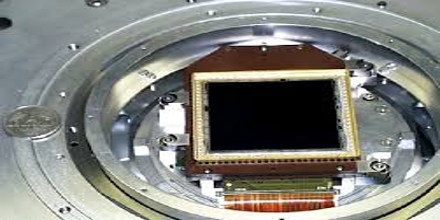
The first working CCD made with integrated circuit technology was a simple 8-bit shift register, reported by Tompsett, Amelio and Smith in August 1970.[10] This device had input and output circuits and was used to demonstrate its use as a shift register and as a crude eight pixel linear imaging device. Development of the device progressed at a rapid rate. By 1971, Bell researchers led by Michael Tompsett were able to capture images with simple linear devices.[11] Several companies, including Fairchild Semiconductor, RCA and Texas Instruments, picked up on the invention and began development programs. Fairchild's effort, led by ex-Bell researcher Gil Amelio, was the first with commercial devices, and by 1974 had a linear 500-element device and a 2-D 100 × 100 pixel device. Steven Sasson, an electrical engineer working for Kodak, invented the first digital still camera using a Fairchild 100 × 100 CCD in 1975.[12]
The interline transfer (ILT) CCD device was proposed by L. Walsh and R. Dyck at Fairchild in 1973 to reduce smear and eliminate a mechanical shutter. To further reduce smear from bright light sources, the frame-interline-transfer (FIT) CCD architecture was developed by K. Horii, T. Kuroda and T. Kunii at Matsushita (now Panasonic) in 1981.[2]
The first KH-11 KENNEN reconnaissance satellite equipped with charge-coupled device array (800 × 800 pixels)[13] technology for imaging was launched in December 1976.[14] Under the leadership of Kazuo Iwama, Sony started a large development effort on CCDs involving a significant investment. Eventually, Sony managed to mass-produce CCDs for their camcorders. Before this happened, Iwama died in August 1982; subsequently, a CCD chip was placed on his tombstone to acknowledge his contribution.[15] The first mass-produced consumer CCD video camera, the CCD-G5, was released by Sony in 1983, based on a prototype developed by Yoshiaki Hagiwara in 1981.[16]
Early CCD sensors suffered from shutter lag. This was largely resolved with the invention of the pinned photodiode (PPD).[2] It was invented by Nobukazu Teranishi, Hiromitsu Shiraki and Yasuo Ishihara at NEC in 1980.[2][17] They recognized that lag can be eliminated if the signal carriers could be transferred from the photodiode to the CCD. This led to their invention of the pinned photodiode, a photodetector structure with low lag, low noise, high quantum efficiency and low dark current.[2] It was first publicly reported by Teranishi and Ishihara with A. Kohono, E. Oda and K. Arai in 1982, with the addition of an anti-blooming structure.[2][18] The new photodetector structure invented at NEC was given the name "pinned photodiode" (PPD) by B.C. Burkey at Kodak in 1984. In 1987, the PPD began to be incorporated into most CCD devices, becoming a fixture in consumer electronic video cameras and then digital still cameras. Since then, the PPD has been used in nearly all CCD sensors and then CMOS sensors.[2]
In January 2006, Boyle and Smith were awarded the National Academy of Engineering Charles Stark Draper Prize,[19] and in 2009 they were awarded the Nobel Prize for Physics,[20] for their invention of the CCD concept. Michael Tompsett was awarded the 2010 National Medal of Technology and Innovation, for pioneering work and electronic technologies including the design and development of the first CCD imagers. He was also awarded the 2012 IEEE Edison Medal for "pioneering contributions to imaging devices including CCD Imagers, cameras and thermal imagers".
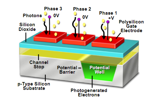
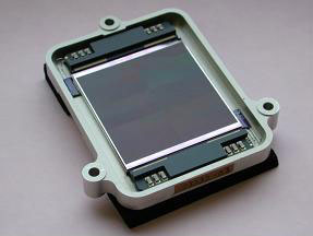
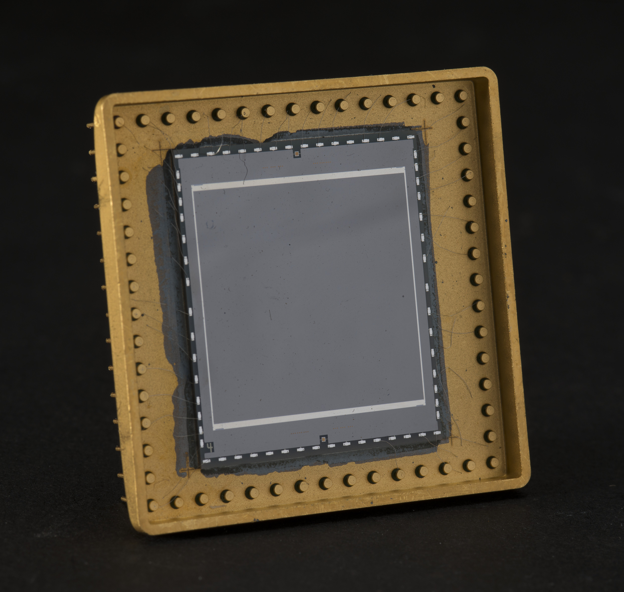
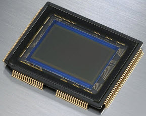
In a CCD for capturing images, there is a photoactive region (an epitaxial layer of silicon), and a transmission region made out of a shift register (the CCD, properly speaking).
An image is projected through a lens onto the capacitor array (the photoactive region), causing each capacitor to accumulate an electric charge proportional to the light intensity at that location. A one-dimensional array, used in line-scan cameras, captures a single slice of the image, whereas a two-dimensional array, used in video and still cameras, captures a two-dimensional picture corresponding to the scene projected onto the focal plane of the sensor. Once the array has been exposed to the image, a control circuit causes each capacitor to transfer its contents to its neighbor (operating as a shift register). The last capacitor in the array dumps its charge into a charge amplifier, which converts the charge into a voltage. By repeating this process, the controlling circuit converts the entire contents of the array in the semiconductor to a sequence of voltages. In a digital device, these voltages are then sampled, digitized, and usually stored in memory; in an analog device (such as an analog video camera), they are processed into a continuous analog signal (e.g. by feeding the output of the charge amplifier into a low-pass filter), which is then processed and fed out to other circuits for transmission, recording, or other processing.[21]
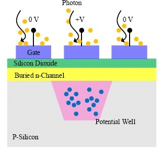
Before the MOS capacitors are exposed to light, they are biased into the depletion region; in n-channel CCDs, the silicon under the bias gate is slightly p-doped or intrinsic. The gate is then biased at a positive potential, above the threshold for strong inversion, which will eventually result in the creation of an n channel below the gate as in a MOSFET. However, it takes time to reach this thermal equilibrium: up to hours in high-end scientific cameras cooled at low temperature.[22] Initially after biasing, the holes are pushed far into the substrate, and no mobile electrons are at or near the surface; the CCD thus operates in a non-equilibrium state called deep depletion.[23] Then, when electron–hole pairs are generated in the depletion region, they are separated by the electric field, the electrons move toward the surface, and the holes move toward the substrate. Four pair-generation processes can be identified:
The last three processes are known as dark-current generation, and add noise to the image; they can limit the total usable integration time. The accumulation of electrons at or near the surface can proceed either until image integration is over and charge begins to be transferred, or thermal equilibrium is reached. In this case, the well is said to be full. The maximum capacity of each well is known as the well depth,[24] typically about 105 electrons per pixel.[23]
The photoactive region of a CCD is, generally, an epitaxial layer of silicon. It is lightly p doped (usually with boron) and is grown upon a substrate material, often p++. In buried-channel devices, the type of design utilized in most modern CCDs, certain areas of the surface of the silicon are ion implanted with phosphorus, giving them an n-doped designation. This region defines the channel in which the photogenerated charge packets will travel. Simon Sze details the advantages of a buried-channel device:[23]
This thin layer (= 0.2–0.3 micron) is fully depleted and the accumulated photogenerated charge is kept away from the surface. This structure has the advantages of higher transfer efficiency and lower dark current, from reduced surface recombination. The penalty is smaller charge capacity, by a factor of 2–3 compared to the surface-channel CCD.
The gate oxide, i.e. the capacitor dielectric, is grown on top of the epitaxial layer and substrate.
Later in the process, polysilicon gates are deposited by chemical vapor deposition, patterned with photolithography, and etched in such a way that the separately phased gates lie perpendicular to the channels. The channels are further defined by utilization of the LOCOS process to produce the channel stop region.
Channel stops are thermally grown oxides that serve to isolate the charge packets in one column from those in another. These channel stops are produced before the polysilicon gates are, as the LOCOS process utilizes a high-temperature step that would destroy the gate material. The channel stops are parallel to, and exclusive of, the channel, or "charge carrying", regions.
Channel stops often have a p+ doped region underlying them, providing a further barrier to the electrons in the charge packets (this discussion of the physics of CCD devices assumes an electron transfer device, though hole transfer is possible).
The clocking of the gates, alternately high and low, will forward and reverse bias the diode that is provided by the buried channel (n-doped) and the epitaxial layer (p-doped). This will cause the CCD to deplete, near the p–n junction and will collect and move the charge packets beneath the gates—and within the channels—of the device.
CCD manufacturing and operation can be optimized for different uses. The above process describes a frame transfer CCD. While CCDs may be manufactured on a heavily doped p++ wafer it is also possible to manufacture a device inside p-wells that have been placed on an n-wafer. This second method, reportedly, reduces smear, dark current, and infrared and red response. This method of manufacture is used in the construction of interline-transfer devices.
Another version of CCD is called a peristaltic CCD. In a peristaltic charge-coupled device, the charge-packet transfer operation is analogous to the peristaltic contraction and dilation of the digestive system. The peristaltic CCD has an additional implant that keeps the charge away from the silicon/silicon dioxide interface and generates a large lateral electric field from one gate to the next. This provides an additional driving force to aid in transfer of the charge packets.
The CCD image sensors can be implemented in several different architectures. The most common are full-frame, frame-transfer, and interline. The distinguishing characteristic of each of these architectures is their approach to the problem of shuttering.
In a full-frame device, all of the image area is active, and there is no electronic shutter. A mechanical shutter must be added to this type of sensor or the image smears as the device is clocked or read out.
With a frame-transfer CCD, half of the silicon area is covered by an opaque mask (typically aluminum). The image can be quickly transferred from the image area to the opaque area or storage region with acceptable smear of a few percent. That image can then be read out slowly from the storage region while a new image is integrating or exposing in the active area. Frame-transfer devices typically do not require a mechanical shutter and were a common architecture for early solid-state broadcast cameras. The downside to the frame-transfer architecture is that it requires twice the silicon real estate of an equivalent full-frame device; hence, it costs roughly twice as much.
The interline architecture extends this concept one step further and masks every other column of the image sensor for storage. In this device, only one pixel shift has to occur to transfer from image area to storage area; thus, shutter times can be less than a microsecond and smear is essentially eliminated. The advantage is not free, however, as the imaging area is now covered by opaque strips dropping the fill factor to approximately 50 percent and the effective quantum efficiency by an equivalent amount. Modern designs have addressed this deleterious characteristic by adding microlenses on the surface of the device to direct light away from the opaque regions and on the active area. Microlenses can bring the fill factor back up to 90 percent or more depending on pixel size and the overall system's optical design.
The choice of architecture comes down to one of utility. If the application cannot tolerate an expensive, failure-prone, power-intensive mechanical shutter, an interline device is the right choice. Consumer snap-shot cameras have used interline devices. On the other hand, for those applications that require the best possible light collection and issues of money, power and time are less important, the full-frame device is the right choice. Astronomers tend to prefer full-frame devices. The frame-transfer falls in between and was a common choice before the fill-factor issue of interline devices was addressed. Today, frame-transfer is usually chosen when an interline architecture is not available, such as in a back-illuminated device.
CCDs containing grids of pixels are used in digital cameras, optical scanners, and video cameras as light-sensing devices. They commonly respond to 70 percent of the incident light (meaning a quantum efficiency of about 70 percent) making them far more efficient than photographic film, which captures only about 2 percent of the incident light.
Most common types of CCDs are sensitive to near-infrared light, which allows infrared photography, night-vision devices, and zero lux (or near zero lux) video-recording/photography. For normal silicon-based detectors, the sensitivity is limited to 1.1 μm. One other consequence of their sensitivity to infrared is that infrared from remote controls often appears on CCD-based digital cameras or camcorders if they do not have infrared blockers.
Cooling reduces the array's dark current, improving the sensitivity of the CCD to low light intensities, even for ultraviolet and visible wavelengths. Professional observatories often cool their detectors with liquid nitrogen to reduce the dark current, and therefore the thermal noise, to negligible levels.
The frame transfer CCD imager was the first imaging structure proposed for CCD Imaging by Michael Tompsett at Bell Laboratories. A frame transfer CCD is a specialized CCD, often used in astronomy and some professional video cameras, designed for high exposure efficiency and correctness.
The normal functioning of a CCD, astronomical or otherwise, can be divided into two phases: exposure and readout. During the first phase, the CCD passively collects incoming photons, storing electrons in its cells. After the exposure time is passed, the cells are read out one line at a time. During the readout phase, cells are shifted down the entire area of the CCD. While they are shifted, they continue to collect light. Thus, if the shifting is not fast enough, errors can result from light that falls on a cell holding charge during the transfer. These errors are referred to as "vertical smear" and cause a strong light source to create a vertical line above and below its exact location. In addition, the CCD cannot be used to collect light while it is being read out. Unfortunately, a faster shifting requires a faster readout, and a faster readout can introduce errors in the cell charge measurement, leading to a higher noise level.
A frame transfer CCD solves both problems: it has a shielded, not light sensitive, area containing as many cells as the area exposed to light. Typically, this area is covered by a reflective material such as aluminium. When the exposure time is up, the cells are transferred very rapidly to the hidden area. Here, safe from any incoming light, cells can be read out at any speed one deems necessary to correctly measure the cells' charge. At the same time, the exposed part of the CCD is collecting light again, so no delay occurs between successive exposures.
The disadvantage of such a CCD is the higher cost: the cell area is basically doubled, and more complex control electronics are needed.
An intensified charge-coupled device (ICCD) is a CCD that is optically connected to an image intensifier that is mounted in front of the CCD.
An image intensifier includes three functional elements: a photocathode, a micro-channel plate (MCP) and a phosphor screen. These three elements are mounted one close behind the other in the mentioned sequence. The photons which are coming from the light source fall onto the photocathode, thereby generating photoelectrons. The photoelectrons are accelerated towards the MCP by an
Porno Celebrities Force
Chubby Dick
Cock Dance
Xvideos Com Big Tits
Natural Boobs Xxx
Charge-coupled device - Wikipedia
Charge-Coupled Device - an overview | ScienceDirect Topics
Introduction to Charge-Coupled Devices (CCDs) | Nikon’s ...
What Is A CCD?- charge coupled device
Устройство с зарядовой связью - Charge-coupled device ...
charge coupled device — с английского на русский
Charge Coupled Device